
Professional PCB manufacturing and assembly
Building 6, Zone 3, Yuekang Road,Bao'an District, Shenzhen, China
+86-13410863085Mon.-Sat.08:00-20:00

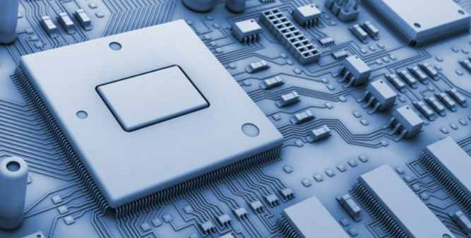
Most PCB wires are copper wires, and the physical characteristics of copper also lead to a certain impedance in the conduction process. The inductance component of wires will affect the transmission of voltage signals, while the resistance component will affect the transmission of current signals. The inductance influence is particularly serious in high-frequency line
1. Reasons for interference of printed wires Printed wires on PCB show resistance or inductive reactance to current respectively in DC or AC state after being energized, and there are inductance effect, resistance effect, conductance effect and mutual inductance effect between parallel wires. A change in the current of one wire must affect the other wire, resulting in interference; PCB board external connection wire or even component lead may become the antenna to transmit or receive interference signals. The DC resistance and AC impedance of the printed wire can be calculated by the formula and formula, R = PL/S and XL = 2πfL formula L is the length of the printed wire (m), s is the cross-sectional area of the wire (mm2), ρ is the resistivity of the copper, TT is a constant, f is the AC frequency. It is because of the existence of these impedance, resulting in a certain potential difference, the existence of these potential differences, will inevitably bring interference, thus affecting the normal work of the circuit.
2. Relation between PCB current and wire width PCB wire width is related to the current carrying value of the circuit. Generally, the wider the wire, the stronger the current carrying capacity. In the actual PCB production process, the wire width should be able to meet the requirements of electrical performance and convenient production is appropriate, its minimum value is determined by the size of the current to withstand, wire width and spacing can be 0.3mm(12mil). The width of the wire should also be considered in the case of high current temperature rise.
Anti-interference design in PCB wirin
3. Wiring in PCB design
In PCB design, wiring is the key stage to the success of PCB design. The position, density, width, spacing and routing form of copper foil conductor on PCB board will determine the anti-interference ability of PCB. Therefore, in order to obtain the best performance of PCB, it must be reasonable wiring.
3.1 Wiring Principles
3.1.1 Plate type selection and density design during wiring
On the premise of meeting the wiring requirements, the PCB layout selection, single panel should be given priority, followed by double panel, multilayer board. Its wiring density, to combine the circuit structure and product performance requirements, reasonable choice, and strive to simple and uniform wiring.

3.1.2 Selection of line width and spacing during wiring
The minimum width of the conductor selected in the PCB is determined by the adhesion strength between the conductor and the insulating substrate
And the value of the current flowing through them. The minimum width and spacing of conductors should not be less than 8mil. If the wiring density allows, the width and spacing of conductors can be widened appropriately. For conductors with copper foil thickness of 2mil and width of 40mil to 600mil, the temperature will not be higher than 3℃ when the current 2A flows through the conductor. Generally, the conductor width of 60mil can meet the requirements. In the absence of special requirements, wiring is usually selected 8 ~ 12mil wire width. For integrated circuits, especially digital circuits, the minimum width of the wire can be selected to reach 2 ~ 2.8mil. In the design, the width of the power supply and ground wire can be widened as far as possible. Generally, the width of the ground wire is greater than that of the power line, and the width of the power line is greater than that of the signal line.
In the design of PCB routing, the input and output wires should avoid crossing as far as possible, and the feedback coupling can be avoided by adding capacitance between the wires. The spacing of wires is generally chosen to be greater than or equal to the line width. The minimum value is determined by the insulation resistance and breakdown voltage between the wires in the worst case. In digital circuits, the spacing can be selected from 5 to 8mil if the process permits.
3.1.3 Selecting a Cabling Mode
The layout of printed conductors shall be as short as possible. When the circuit is high frequency circuit or wiring dense case, printed wire turning should be rounded. When the printed wire turns into a right Angle or sharp Angle, the electrical characteristics of the circuit will be affected in the case of high frequency circuit or wiring density. In PCB design, because the right Angle or included Angle will affect the electrical performance in the high frequency circuit, the wire turning generally uses 45 degree polyline or circular arc, generally does not use 90 degree polyline wiring. When wiring on both sides, PCB double-sided wires generally choose orthogonal vertical, oblique or curved routes to avoid parallel to each other, so as to reduce parasitic coupling between boards.


Just upload Gerber files, BOM files and design files, and the KINGFORD team will provide a complete quotation within 24h.