
Professional PCB manufacturing and assembly
Building 6, Zone 3, Yuekang Road,Bao'an District, Shenzhen, China
+86-13410863085Mon.-Sat.08:00-20:00


Copper coating refers to the area without wiring on the PCB board covered with copper foil, connected with the ground wire, in order to increase the ground wire area, reduce the loop area, reduce voltage drop, improve power efficiency and anti-interference ability. Copper coating can not only reduce the ground impedance, but also reduce the cross-sectional area of the loop and enhance the mirror loop of the signal. Therefore, copper coating process plays a very key role in PCB process, incomplete, truncated mirror loop or incorrect position of copper layer often lead to new interference, have a negative impact on the use of the board.
DPC substrate preparation process
DPC base structure
Comparison of copper coating process and thick film process
LAM process and DPC process
In the LAM process, ceramic metallization uses high energy laser beam to formalize ceramic and metal ions, so that the two are closely combined to achieve the effect of growing together. LAM technology of copper coating, with copper layer thickness controllable, graphic accuracy easy to control and other advantages, Silitong ceramic circuit board copper coating thickness can be customized according to customer requirements between 1μm ~ 1mm, line width, line diameter can do 20μm. That is to say, with the application and deepening of science and technology in the laser field, the copper coating technology of PCB industry has been able to achieve the effect of high bonding degree between ceramic and metal layer and excellent performance through laser technology.
In DPC process, electroplating process is adopted. Ceramic metallization generally adopts sputtering process to form adhesion layer with chromium or titanium as material and seed layer with copper as material on ceramic surface successively. Adhesion layer can increase the adhesion strength of metal lines, while copper seed layer plays the role of conductive layer.
Through the above analysis of the parasitic characteristics of the holes, we can see that in the design of high-speed PCB, seemingly simple holes often bring great negative effects to the circuit design. In order to reduce the adverse effects brought by the parasitic effect of the hole, the design can be as far as possible:
1, from the cost and signal quality, choose a reasonable size of the hole size. For example, for the design of 6-10 layers of memory module PCB, it is better to choose 10/20Mil (drill/pad) pass hole, for some high-density small size boards, you can also try to use 8/18Mil pass hole.

With current technology, it is difficult to use smaller holes. For the power supply or ground wire hole can be considered to use a larger size, to reduce the impedance.
2. From the two formulas discussed above, it can be concluded that the use of thinner PCB board is beneficial to reduce the two parasitic parameters through the hole.
3. The signal routing on the PCB board should not be changed as far as possible, that is to say, try not to use unnecessary holes.
4. The pins of the power supply and the ground should be drilled nearby. The shorter the lead between the pins and the holes, the better, because they will lead to the increase of inductance. At the same time, power and ground leads should be as thick as possible to reduce impedance.
5. Place some grounded holes near the holes of the signal changing layer in order to provide the nearest loop for the signal. You can even put a lot of extra ground holes on the PCB board. Of course, you need to be flexible in your design. The perforated model discussed above is the case that each layer has pads, and sometimes, we can reduce or even remove the pads of some layers.
6. Especially in the case of very large pore density, it may lead to the formation of a cut off circuit slot in the copper layer. To solve this problem, in addition to moving the position of the hole, we can also consider reducing the size of the solder pad in the copper layer.
It can be seen from the formula that the diameter of the through hole has little influence on the inductance, while the length of the through hole has the biggest influence on the inductance. Using the above example again, the inductance of the hole can be calculated as:
L = 5.08 x0.050 [ln (4 x0. 050/0.010) + 1)
= 1.015 nH
If the rise time of the signal is 1ns, its equivalent impedance is:
XL = = 3.19 Ω PI L/T10-90
Such impedance can no longer be ignored in the presence of high frequency current. In particular, note that the bypass capacitor needs to pass through two holes when connecting the power layer to the formation, so that the parasitic inductance of the holes will be multiplied.
The technique of designing through holes

The composition of the pores
May 14,2023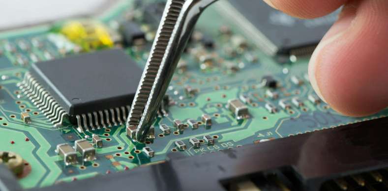


Just upload Gerber files, BOM files and design files, and the KINGFORD team will provide a complete quotation within 24h.