
Professional PCB manufacturing and assembly
Building 6, Zone 3, Yuekang Road,Bao'an District, Shenzhen, China
+86-13410863085Mon.-Sat.08:00-20:00


Monolithic RF devices greatly facilitate the application of wireless communication in a certain range. A complete wireless communication link can be formed by using appropriate microcontroller and antenna combined with the transceiver device. They can be integrated on a small circuit board, used in wireless digital audio, digital video data transmission system, wireless remote control and telemetry system, wireless data acquisition system, wireless network and wireless security system and many other fields.
How to plan and design radio frequency and digital circuits on PCB board?
1. Potential contradiction between digital circuit and analog circuit
If the analog (RF) and digital (microcontroller) circuits work well on their own, but if you put them on the same circuit board and use the same power supply together, the whole system is likely to be unstable. This is mainly because the digital signal frequently oscillates between the ground and the positive power supply (size 3V), and the period is particularly short, often ns level. Due to the large amplitude and small switching time, these digital signals contain a large number of high frequency components independent of switching frequency. In the analog part, the signal from the antenna tuning loop to the receiving part of the wireless device is generally less than 1μV. So the difference between digital and RF signals will be 10-6 (120dB). Obviously, if the digital signal is not well separated from the RF signal, the weak RF signal may be damaged, and the wireless device performance will deteriorate or even not work at all.

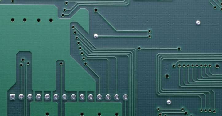
2, RF circuit and digital circuit do in the same block PCB common problems
Inadequate isolation of sensitive and noisy signal lines is a frequent problem. As mentioned above, digital signals have high swing and contain a large number of high frequency harmonics. If the digital signal wiring on the PCB board is adjacent to sensitive analog signals, high frequency harmonics may be coupled past. The most sensitive nodes of RF devices are usually the loop filter circuit of the phase-locked loop (PLL), the external voltage controlled oscillator (VCO) inductor, the crystal reference signal, and the antenna terminals. These parts of the circuit should be treated with special care.
(1) Power supply noise
Since the input/output signal has a swing of several volts, digital circuits are generally acceptable for power noise (less than 50mV). However, analog circuits are quite sensitive to power supply noise, especially to burr voltage and other high frequency harmonics. Therefore, power line wiring on PCB boards containing RF (or other analog) circuits must be more careful than on ordinary digital boards and automatic wiring should be avoided. It should also be noted that the microcontroller (or other digital circuit) will suddenly suck in most of the current for a short time during each internal clock cycle, due to the CMOS process design used in modern microcontrollers. Thus, assuming that a microcontroller operates at an internal clock frequency of 1MHz, it will extract (pulse) current from the power supply at this frequency, which will certainly cause voltage burrs on the power line if proper power decoupling is not applied. If these voltage burrs reach the power supply pins in the RF part of the circuit, they may seriously cause work failure. Therefore, it is necessary to ensure that the analog power line is separated from the digital circuit area.
(2) Unreasonable ground wire
RF circuit boards should always be covered with a ground layer connected to the negative terminal of the power supply, which may produce some strange phenomena if not handled properly. This may be difficult for a digital circuit designer to understand, because most digital circuits function well even without the grounding layer. In the RF band, even a short wire acts like an inductor. By rough calculation, the inductance per mm length is about 1nH, and the inductance of a 10mmPCB line at 434MHz is about 27Ω. If the ground layer is not used, most ground wires will be longer and the circuit will not guarantee the design characteristics.
(3) Antenna radiation to other analog parts
This is often overlooked in circuits that contain RF and other components. In addition to the RF portion, there are usually other analog circuits on the board. For example, many microcontrollers have built-in analog-to-digital converters (ADCs) that measure analog inputs as well as battery voltage or other parameters. If the RF transmitter's antenna is located near (or on) this PCB, the emitted high-frequency signal may reach the analog input of the ADC. Don't forget that any electrical circuit may act as an antenna to send or receive RF signals. If the ADC input processing is not reasonable, the RF signal may be self-excited in the ESD diode input ADC, resulting in ADC deviation.


Just upload Gerber files, BOM files and design files, and the KINGFORD team will provide a complete quotation within 24h.