
Professional PCB manufacturing and assembly
Building 6, Zone 3, Yuekang Road,Bao'an District, Shenzhen, China
+86-13410863085Mon.-Sat.08:00-20:00


Nine rules of high speed PCB design to solve EMI problems
With the decrease of signal rising time and the increase of signal frequency, the EMI problem of electronic products will be more and more noticed by electronic engineers. With the success of high-speed PCB design, the contribution to EMI has been paid more and more attention. Almost 60% EMI problems can be controlled and solved by high-speed PCB. I have done EMI design for 4 years, and I have some ideas to communicate with you.
Rule 1 Rules for masking high-speed signal cabling
As shown in the figure above: In high-speed PCB design, key high-speed signal lines such as clocks need to be screened for routing. If no shielding or only partial shielding is done, EMI leakage will be caused. It is recommended that shielded cables be drilled and grounded every 1000mil.
Rule 2. Closed-loop routing rules for high-speed signals
Due to the increasing density of PCB board, it is easy for many PCB LAYOUT engineers to make such mistakes in the process of wiring, as shown in the figure below:
Due to the increasing density of PCB board, it is easy for many PCB LAYOUT engineers to make a mistake in the process of wiring, that is, high-speed signal network such as clock signal generates a closed-loop result when multi-layer PCB is wiring. Such closed-loop result will generate a ring antenna and increase the radiation intensity of EMI.
Rule 3 Open loop rule for high-speed signal routing
Rule two mentions that a closed loop of a high-speed signal will cause EMI radiation, while an open loop will also cause EMI radiation.
High-speed signal networks, such as clock signals, will generate linear antennas and increase EMI radiation intensity once the open-loop result is generated during the wiring of multi-layer PCB.
Rule IV. Characteristic impedance continuity rules for high-speed signals

High-speed signals must ensure the continuity of characteristic impedance when switching between layers, otherwise EMI radiation will be increased. In other words, the width of the wiring in the same layer must be continuous, and the impedance of the different layers must be continuous.
Rule five Routing direction rules for high speed PCB design
The cables between two adjacent layers must be routed vertically. Otherwise, cross-talk will occur between the two layers and EMI radiation will be increased.
In short, adjacent wiring layers follow the direction of horizontal, horizontal and vertical, and vertical wiring can suppress crosstalk between lines.
Rule 6 Topological structure rules in high speed PCB design
In high speed PCB design, the circuit board characteristic impedance control and multi-load topology design directly determine the success or failure of the product.
The Daisy chain topology is shown here, which is generally used for the benefit of a few Mhz. It is recommended to use the star symmetrical structure at the back end in high speed PCB design.
Rule 7 Resonance rule for cable length
Check whether the length of the signal line and the frequency of the signal constitute resonance, that is, when the length of the wiring is an integer multiple of the signal wavelength of 1/4, the wiring will generate resonance, and the resonance will radiate electromagnetic waves, resulting in interference.
Rule eight Rules for reflux path
All high speed signals must have a good return path. As far as possible, the return path of high-speed signal such as clock is small. Otherwise, it will greatly increase the radiation, and the radiation size is proportional to the area surrounded by the signal path and the return path.
Rule nine: Device decoupling capacitor placement rules
The location of the decoupling capacitor is very important. Improper placement does not have the effect of decoupling. The principle is: close to the pin of the power supply, and the area surrounded by the power supply and ground is small.
Iii. Summary and reason analysis of high-speed PCB design rules
The clock frequency of 1PCB is more than 5MHZ or the signal rise time is less than 5ns, which generally requires the use of multilayer design.
Reason: Using multilayer board design signal loop area can be well controlled.
2 For multilayer board, key wiring layer (clock line, bus,
After careful consideration and prediction, the design of online circuit testing can be carried out at the initial stage of design and implemented later in the production process. The type of through-hole fan-out can be determined according to the wiring path and online circuit testing. The power supply and grounding will also affect the wiring and fan-out design. In order to reduce the inductive reactance generated by the connection line of the filter capacitor, the pass hole should be as close as possible to the pin of the surface-mounted device. If necessary, manual wiring can be used, which may affect the original thought of the wiring path, or even cause you to reconsider which kind of pass hole to use. Therefore, the relationship between the pass hole and the pin inductive reactance must be considered and the priority of the pass hole specification must be set.

Basic design process
May 10,2023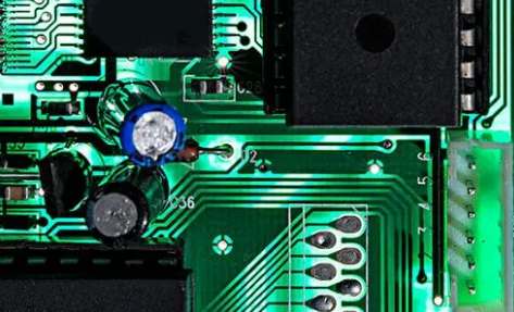


Just upload Gerber files, BOM files and design files, and the KINGFORD team will provide a complete quotation within 24h.