
Professional PCB manufacturing and assembly
Building 6, Zone 3, Yuekang Road,Bao'an District, Shenzhen, China
+86-13410863085Mon.-Sat.08:00-20:00

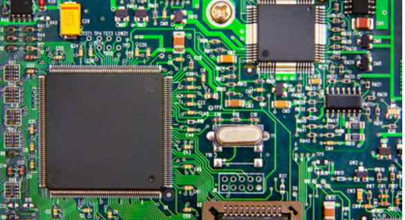
Ordinary FR4 does not achieve very reliable electrical performance, but high performance FR4 materials do have good reliable characteristics, such as higher Tg, are still relatively low cost, and can be used in a wide variety of applications, from simple audio design to complex microwave applications.
Rf/microwave design considerations
Portable technology and Bluetooth pave the way for RF/microwave applications in wearable devices. Today's frequency range is becoming more dynamic. Just a few years ago, very high frequency (VHF) was defined as 2GHz to 3GHz. But now we can see ultra-high frequency (UHF) applications in the range of 10GHz to 25GHz.
Therefore, for wearable PCBS, the RF component requires closer attention to the wiring, separating the signals separately and keeping the high frequency signals away from the ground. Other considerations include providing a by-pass filter, adequate decoupling capacitance, grounding, and designing the transmission line and return route to be nearly equal.
The bypass filter can suppress the ripple effect of noise content and crosstalk. The decoupling capacitor needs to be placed closer to the pin of the device carrying the power signal.
High-speed transmission lines and signal loops require a layer between the power layer signals to smooth out the jitter generated by noisy signals. At higher signal speeds, even small impedance mismatches can result in unbalanced transmission and reception, resulting in distortion. Therefore, special attention must be paid to impedance matching problems related to RF signals, which have high speeds and special tolerances.
Rf transmission lines require controlled impedance in order to transmit RF signals from a specific IC base to the PCB. These transmission lines can be implemented in the outer, top and bottom layers, or they can be designed in the middle layer.
Methods used during PCB RF design layouts are microstrip lines, suspended strip lines, coplanar waveguides, or ground. The microstrip line consists of a fixed length of metal or wire and the whole or part of the ground plane located directly below it. Characteristic impedances in general microstrip line structures range from 50Ω to 75Ω.
Figure 2: Coplanar waveguides provide better isolation near RF lines and lines that need to be routed very close together

The suspended strip line is another method of wiring and noise suppression. This line consists of a fixed width wiring on the inner layer and a large ground plane above and below the center conductor. The ground plane is sandwiched between the power layer and thus provides very effective grounding. This is an optimal method for RF signal wiring of wearable PCB.
Coplanar waveguides can provide better isolation near RF lines and lines that need to be routed close to them. This medium consists of a central conductor and a ground plane on either side or below. The best method for transmitting RF signals is a suspended ribbon or coplanar waveguide. These two methods provide better isolation between signal and RF wiring.
A so-called "through-hole fence" is recommended on either side of a coplanar waveguide. This method provides a row of ground through holes in each metal ground plane of the central conductor. The main lines running in the middle are fenced on each side, thus giving the return current a shortcut to the ground below. This method can reduce the noise levels associated with the high ripple effect of the RF signal. The permittivity of 4.5 remains the same as that of the semi-cured sheet FR4 material, while the permittivity of the semi-cured sheet -- from microstrip, strip, or offset strip lines -- is about 3.8 to 3.9.
Figure 3: The use of through-hole fences is recommended on either side of the coplanar waveguide
In some devices that use the ground plane, blind holes may be used to improve decoupling performance of the power supply capacitance and to provide a shunt path from the device to the ground. The shunt path to ground shortens the length of the through-hole, which serves two purposes: not only do you create a shunt or ground, but you reduce the transmission distance of devices with small fields, an important RF design factor.


Just upload Gerber files, BOM files and design files, and the KINGFORD team will provide a complete quotation within 24h.