
Professional PCB manufacturing and assembly
Building 6, Zone 3, Yuekang Road,Bao'an District, Shenzhen, China
+86-13410863085Mon.-Sat.08:00-20:00

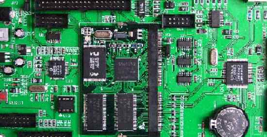
In the process of PCB board, there will be a lot of accidents, such as copper plating, electroless copper plating, gold plating, tinned lead alloy coating layer. So what causes this stratification? Next, Shenzhen PCB Board Factory - Shenzhen kingford will analyze the reasons for PCB plating and stratification.
Cause analysis of PCB board plating stratification
Under ultraviolet irradiation, the photoinitiator which absorbed the light energy was decomposed into free group initiator monomer for photopolymerization reaction, forming the shape molecule which was insoluble in dilute alkali solution. Under exposure, due to incomplete polymerization, in the development process, the film swelling and softening, resulting in unclear lines and even film falling off, resulting in poor combination of film and copper; If the exposure is excessive, it will cause difficulties in development, and it will also produce warping peeling in the plating process, forming osmotic plating.
So it's important to control your exposure energy; After the surface of copper is treated, the cleaning time is not easy to be too long, because the cleaning water also contains a certain acidic substance although its content is weak, but the influence of the surface of copper can not be taken lightly, should be strictly in accordance with the PCB process specifications for cleaning operations.
The main reason why the gold layer falls off from the surface of the nickel layer is the surface treatment of nickel. The poor surface activity of nickel metal is difficult to obtain satisfactory results. Nickel coating surface is easy to produce passivation film in the air, such as improper treatment, will make the gold layer from the nickel layer surface separation. Such as improper activation in the electroplating, the gold layer will be removed from the surface of the nickel layer that peeling off. The second reason is that after activation, cleaning time is too long, resulting in nickel surface passivation film formation, and then to gilding, coating is bound to fall off defects.
In fact, there are many reasons for the plating stratification. If you want to avoid similar situations in the process of PCB board making, it is important to the care and responsibility of technical personnel. Therefore, an excellent PCB manufacturer will conduct high-standard training for every workshop employee to prevent the delivery of inferior products.

2.PCB design component arrangement rules
PCB design layout also contains a great deal of knowledge. At present, there are five common principles in PCB design, which are the rule of component arrangement, the principle of layout according to the signal direction, the principle of electromagnetic interference prevention, the principle of thermal interference suppression and the principle of adjustable component layout. Today we will first introduce the PCB design component arrangement rules.
PCB design element arrangement rules
1. Under normal conditions, all components should be arranged on the same surface of the printed circuit. Only when the top component is too dense, can some highly limited and small heat devices, such as patch resistance, patch capacitor, patch IC, etc. be placed on the bottom.
2. Under the premise of ensuring electrical performance, components should be placed on the grid and arranged parallel or vertical to each other, in order to neat and beautiful, generally do not allow components overlap; Element arrangement should be compact, input and output components as far away as possible.
3. There may be a high potential difference between a component or wire, should increase their distance, so as to avoid accidental short circuit caused by discharge, breakdown.
4. The components with high voltage should be arranged as far as possible in the place where the hand is not easy to touch when debugging.
5. Components located at the edge of the plate, at least 2 plate thickness away from the edge of the plate.
6. Components on the whole board surface should be evenly distributed, consistent density.
This is the component arrangement rules in PCB design and layout, which can clearly see that the PCB board on the component arrangement is not arbitrary, seen in many exhibitions, various shapes of PCB board are specially adjusted by technical personnel, otherwise it will lead to the circuit board can not operate. Therefore, we must be very careful when designing PCB circuit, must not blindly pursue novel and unique oh.
Shenzhen kingford mPCB boardaking ability
Energy production from 2 layers to 14 layers, 14-22 layers can be proofing production.
Minimum line width/spacing: 3mil/3milBGA Spacing :0.20MM
Minimum aperture: 0.1mm Size :610mmX1200mm
Ink: Tamura, Taiyo, Fudoken;
FR4: Shengyi, Kingboard, Harbour, Hongren, Guoji, Hezheng, Nanya,
(Shengyi S1130/S1141/S1170),Tg130℃/ Tg170℃ T g180℃ and other high TG plates)
High frequency plate: Rogers, Taconic, ARLLON;
Surface process: tin spray, lead-free tin spray, gold plating, full plate gold plating, plug gold plating, full plate thick gold, chemical tin (silver), anti-oxidation (OSP) blue glue, carbon oil.
Shenzhen kingford PCBA processing advantages
1. Highly professional: The company focuses on processing samples and small and medium-sized batches, and promises to deliver the materials within 3-5 working days after confirmation.
2. Professional equipment: The company's equipment is tailored for sample and small and medium-sized batch production of advanced equipment, can stick 0201, BGA spacing 0.3MM, QFN, CSP, CON and other components.
3. Professional technology: 100% of technical backbone workers have more than 5 years of work experience, 85% of front-line operators have more than 3 years of work experience.
4. The company implements the 5S and 6σ concepts in daily operation, so as to ensure that the shipment is checked at least 7 times. If the quantity reaches 100PCS, our company promises to pass AOI optical inspection.
5. The company promises that the straight through rate of welding is more than 99%. If customers find welding defects, the company promises to repair them free of charge.


Just upload Gerber files, BOM files and design files, and the KINGFORD team will provide a complete quotation within 24h.