
Professional PCB manufacturing and assembly
Building 6, Zone 3, Yuekang Road,Bao'an District, Shenzhen, China
+86-13410863085Mon.-Sat.08:00-20:00

PCB copying board backloading schematic is a common project in PCB copying board business. kingford is a professional PCB copying board company with many years of actual experience in PCB copying board. Kingford can provide one-stop PCB copying board solutions such as board modification, schematic copying, chip model identification, chip decryption, PCB copying board proofing, PCBA OEM and material replacement. Next, we will introduce the PCB board back push schematic method.
What is PCB copy board?
PCB copy board, the industry is also often referred to as board copy board, board clone, board copy, PCB clone, PCB reverse design or PCB reverse research and development. In other words, on the premise of existing physical electronic products and circuit boards, reverse analysis of circuit boards is carried out by using reverse R&D technology means, and the original product's PCB file, bill of materials (BOM) file, schematic file and other technical documents as well as PCB silkscreen production files are 1:1 restoration. Then use these technical documents and production documents to make PCB board, component welding, fly needle testing, circuit board debugging, and complete the complete copy of the original circuit board template.
Use of PCB copy board
For PCB copy board, many people do not understand, in the end what is PCB copy board, some people even think PCB copy board is copycat. But PCB copying board is definitely not imitating. The purpose of PCB copying board is to learn the latest foreign electronic circuit design technology, and then absorb the excellent design scheme, and then used to develop and design more excellent products.
With the continuous development and deepening of the board copying industry, today's PCB board copying concept has been extended to a wider range, is no longer limited to simple circuit board copying and cloning, but also involves the secondary development of products and the research and development of new products.
For example, through the analysis of existing product technical documents, the understanding and discussion of design ideas, structural features and process technology, it can provide feasibility analysis and competitive reference for the research and development design of new products, assist research and development design units to timely follow up the latest technological development trend, timely adjust and improve product design schemes, and develop the most competitive new products in the market.
Through the extraction and partial modification of the technical data files, the process of PCB board copying can realize the rapid update and upgrade of various types of electronic products and secondary development. According to the document drawing and schematic diagram extracted from the board copying, professional designers can also optimize the design and change the PCB board according to the wishes of customers. On this basis, new functions can be added to the product or functional features can be redesigned. In this way, the product with new functions will appear in the fastest speed and new attitude. It not only owns its own intellectual property rights, but also wins the opportunity in the market, bringing double benefits to customers.
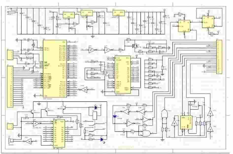
Whether it is used to analyze circuit board principles and product performance in reverse research, or reused as the basis and basis of PCB design in forward design, PCB schematics have a special role.
PCB copy board backsliding schematic method
1. Record the PCB details
Get a PCB, first of all on the paper record the model, parameters, and position of all components, especially the diode, the direction of the three-stage tube, the direction of the IC notch. It's best to take two pictures of the device's location with a digital camera. A lot of pcb circuit boards do more advanced above the diode transistor some do not pay attention to see.
2. Scanned image
Remove all the components and remove the tin from the PAD hole. The PCB is cleaned with alcohol and placed in a scanner, which scans with slightly higher pixels to get a sharper image. Then the top and bottom layers are lightly polished with gauze paper until the copper film shines, put them in the scanner, start PHOTOSHOP, and sweep the two layers in color separately.
Note that PCB must be placed horizontally and vertically in the scanner, otherwise the scanned image cannot be used.
3. Adjust and correct the image
Adjust the contrast and brightness of the canvas so that the part with copper film is in strong contrast with the part without copper film, then turn the subdrawing to black and white, check whether the lines are clear, if not, repeat this step. If it is clear, save the picture as black and white BMP format files TOP BMP and BOT BMP. If there is any problem with the picture, you can use PHOTOSHOP to repair and correct it.
4. Verify the position compatibility between the PAD and VIA
The two BMP files are converted into PROTEL files respectively, and two layers are transferred into PROTEL. If the positions of PAD and VIA after two layers are basically identical, it indicates that the previous steps have been done well. If there is any deviation, repeat the third step. So pcb copying board is a very patient work, because a little problem will affect the quality and the degree of matching after copying board.
5. Draw layers
Convert the BMP of the TOP layer to the TOP PCB, be careful to convert to the SILK layer, which is the yellow layer. Then you trace the line on the TOP layer and place the device according to the drawing of step 2. Delete the SILK layer when you are done. Repeat until all layers are drawn.
6. Record the PCB details
TOP PCB and BOT PCB are combined

7. Laser print the TOP LAYER and BOTTOM LAYER
Use a laser printer to print the TOP LAYER and BOTTOM LAYER onto the transparent film (1:1 ratio), place the film on the PCB, compare and see if it's wrong, if it's right, you're done.
Step 8 Test
Test copy board electronic technology performance is the same as the original board. If it's one, it's really done.
PCB copy board push-back schematic pay attention to details
1. Divide functional areas reasonably
In the reverse design of a good PCB circuit board schematic, reasonable division of functional areas can help engineers reduce some unnecessary trouble and improve the efficiency of drawing.
Generally speaking, the components with the same function on a PCB board will be centrally arranged, and the functional division of the area can be a convenient and accurate basis for the backdrawing of the schematic. However, the division of this functional area is not arbitrary. It requires engineers to have some knowledge of electronic circuits.
First, find out the core components in a certain functional unit, and then find out other components of the same functional unit according to the wiring connection, and form a functional partition (the formation of functional partition is the basis of schematic drawing). Also, during this process, don't forget to use the component numbers on the circuit board, which can help you partition functions faster.
2. Find the correct benchmark
This reference piece can also be said to be the main component PCB network city at the beginning of schematic drawing. After determining the reference piece, drawing according to the pins of these reference pieces can ensure the accuracy of schematic diagram to a greater extent.
For engineers, the determination of the reference is not a very complex thing, in general, you can choose to play a major role in the circuit components as the reference, they are generally larger, more pins, easy to draw, such as integrated circuit, transformer, transistor and so on, can be used as a suitable reference.
3. Correctly distinguish lines and reasonably draw wiring
For the distinction of ground wire, power cord and signal line, engineers also need to have relevant knowledge of power supply, circuit connection knowledge, PCB wiring knowledge and so on. The distinction of these lines can be analyzed from the connection of components, the width of copper foil and the characteristics of the electronic products themselves.
In wiring drawing, in order to avoid crossing and interspersing lines, a large number of ground symbols can be used for ground wires. Different lines of different colors can be used to ensure clear identification. Special marks can also be used for various components, and unit circuits can even be drawn separately and then combined.
4. Master the basic framework and draw lessons from similar schematic diagrams
For some basic electronic circuit framework and schematic method, engineers need to master, not only to be able to draw some simple and classic basic cell circuit composition form directly, but also to form the overall framework of electronic circuit.
On the other hand, do not ignore that the schematic diagram of the same type of electronic products has certain similarities to PCB network city, engineers can fully draw lessons from the similar circuit diagram according to the accumulation of experience to carry out the new product schematic backsliding.
5. Check and optimize
After the schematic drawing is completed, the reverse design of PCB schematic diagram can be concluded only after testing and checking. The nominal values of components sensitive to PCB distribution parameters need to be checked and optimized. The schematic diagram is compared, analyzed and checked according to the PCB file diagram to ensure that the schematic diagram is completely consistent with the file diagram.
kingford PCB copying ability
Number of top floors: 38;
Maximum plate thickness: 6 mm ±0.05 mm(2 mil);
Maximum size: 640 mm × 480 mm ±0.1 mm(4 mil);
Minimum line width: 0.01mm (0.4mil) for hard plate / 0.005mm (0.2mil) ± 0.01mm (0.4mil) for flexible plate;
Minimum line clearance: hard plate 0.01mm (0.4mil)/ flexible plate 0.005mm (0.2mil) ± 0.01mm (0.4mil);
Minimum mechanical through-hole: 0.15 mm(6 mil) hard plate / 0.1 mm(4 mil) ±0.01 mm(0.4 mil) flexible plate;
Minimum mechanical holes: 0.15 mm(6 mil) for hard plate / 0.1 mm(4 mil) ±0.01 mm(0.4 mil) for flexible plate;
Minimum blind hole: hard plate 0.1mm (4 mil)/flexible plate 0.1mm (4 mil) ± 0.01mm (0.4mil);
Minimum laser hole: hard plate 0.1mm (4 mil)/flexible plate 0.1mm (4 mil) ± 0.01mm (0.4mil);
Blind hole types: 1st order, 2nd order, 3rd order, 4th order laser blind hole;
Type of buried hole: > 20 categories;
Multilayer copper thickness measurement: ± 1.7um (0.05oZ);
Multilayer thickness measurement: ±5 um(0.2 mil);
Impedance measurement: 5 ~ 150 Ω ±0.5Ω;
Resistance value measurement: 0.000001Ω ~ 20 MΩ ±5%;
Capacitance measurement: 0.001pF ~ 100F ±5%;
Inductance measurement: 0.001nH ~ 10H ±5%;
Magnetic bead equivalent resistance measurement: 10Ω ~ 2000 Ω(100MHz) ±10%;
Crystal frequency measurement: 1KHz ~ 200MHz ±1%;
Voltage regulator diode measurement: 0.5V ~ 56V ±0.01V.
PCB copy board service process
1. Customer provides product pictures or sample copy board;
2. Evaluate quotation according to pictures or samples and customer needs;
3. The customer confirms the quotation, signs the contract and pays the project deposit;
4. Received advance payment and arranged engineers to copy the board;
5. After copying the board, provide the screenshot of the document to the customer for confirmation;
6. The customer confirmed OK, settled the balance, and provided the information of copying the board.


Just upload Gerber files, BOM files and design files, and the KINGFORD team will provide a complete quotation within 24h.