
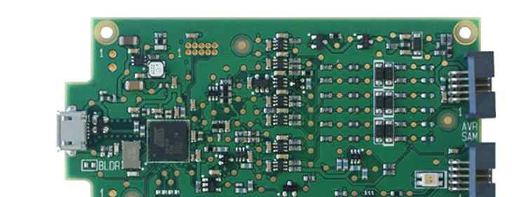
Professional PCB manufacturing and assembly
Building 6, Zone 3, Yuekang Road,Bao'an District, Shenzhen, China
+86-13410863085Mon.-Sat.08:00-20:00

PCB board also has shelf life, after vacuum packaging should be processed in time, can not be kept for a long time, PCBA processing beyond the storage period of PCB board factory will cause harm to PCB board, next, Shenzhen PCBA processing manufacturer -kingford will introduce the three hazards of using expired PCB board in PCBA processing.
PCBA processing using the three hazards of expired PCB board
1, PCBA processing using expired PCB may cause oxidation of PCB surface welding pad
The oxidation of the pad will cause solder defects, which may eventually lead to functional failure or loss of parts. Different surface treatment of the circuit board for the effect of oxidation will not be the same, in principle ENIG requirements to be used up within 12 months, and OSP is required to be used up within six months, it is recommended that in accordance with the PCB board factory shelflife (shelflife) to ensure quality.
Generally, the OSP board can be sent back to the board factory to wash off the OSP film and then put on a new layer of OSP. However, the copper foil line may be damaged when the OSP is removed by pickling. Therefore, it is best to consult the board factory to confirm whether the OSP film can be reprocessed.
ENIG plate can not be re-processed, the general recommendation is to "press roast", and then test whether there is a problem.
2, PCBA processing using expired PCB may cause moisture absorption and explosion board
When the board is backsoldered after absorbing moisture, it may cause problems such as popcorn effect, exploding board or delamination. This problem can be solved by baking, but not every board is suitable for baking, and baking may cause other quality problems.
Generally speaking, OSP board is not recommended to bake, because high temperature baking will damage the OSP film, but also have seen some people will take OSP to bake, but the baking time should be as short as possible, the temperature can not be too high, after baking more must be completed in the shortest time back welding furnace, many challenges, otherwise the welding pad will appear oxidation, affect welding.
3, PCBA processing using expired PCB bonding ability may degrade and deteriorate
After the circuit board is produced, the bonding ability between layers will gradually degrade or even deteriorate over time. That is to say, as time goes on, the bonding force between layers of the circuit board will gradually decline.
Such a circuit board after the high temperature of the backwelding furnace, because the circuit board composed of different materials will have different coefficient of thermal expansion, under the action of thermal expansion and contraction, it is possible to cause the circuit board delamination (de-lamination), surface bubbles, which will seriously affect the reliability and long-term reliability of the circuit board, Because the circuit board layer may break the circuit board layer between the conduction hole (via), resulting in poor electrical characteristics, the most troublesome is the possibility of intermittent poor problems, more likely to cause CAF (micro short circuit) without awareness.
The harm of using expired PCB is quite big, so the PCBA processing should use the PCB board within the shelf life.
2. How to distinguish SMT patch resistance, capacitance and inductance?
Patch resistance parts are widely used in consumer electronics, small equipment products, automotive electronic products. With the demand of thin and miniaturization of electronic products, the size precision of patch resistance and tolerance parts is getting higher and higher. In 2018, the minimum patch resistance size is 01005. The commonly used patch resistance, patch inductance and patch capacitance are difficult to distinguish in appearance. Next, we will introduce how SMT patch machining can distinguish patch resistance, capacitance and inductance.
SMT patch processing patch resistance and patch capacitance resolution method
1. Look at the color - all the capacitors of the patch are not silk-printed, since the production process is sintering at low temperature, but printing on the outside. Its color is mostly cyan gray.
2. Look at the mark -- the symbol of the patch capacitor in the circuit is "C", and the symbol of the patch resistance is "R".
3. Look at the silk screen - the unusual feature of silk screen is usually resistance.
Method for separating SMT chip capacitance and chip inductance
1. Look at the color -- unusual usually, as long as the tantalum capacitor of the patch is black, the other is not black at all. And the patch inductors are all black.
2. Look at the model code -- the chip inductance starts with L, and the chip capacitance starts with C. From the shape is round beginning to conclude that should be inductance.
3. Look at the external layout -- find the same components can or split components to see the external layout, with coil layout for the chip inductor.
SMT patch processing and patch inductance resolution method
1. According to the shape -- the shape of the inductance has a multilateral shape, and the resistance is mainly rectangular. Especially when it is round, the anomaly is usually identified as inductance.
2. The resistance value of the measurement -- the resistance value of the inductor is relatively small, and the resistance value of the resistance is relatively large.
Choose Shenzhen kingford to do PCBA processing four reasons
1. Strength guarantee
▪SMT workshop: We have imported SMT machines and several sets of optical inspection equipment, with a daily output of 4 million. Each process is equipped with QC personnel, who can keep an eye on product quality.
▪DIP production line: We have two wave-soldering machines, among which there are more than 10 old employees who have worked for more than three years. The skilled workers can weld all kinds of plug-in materials.
2. Quality assurance, cost-effective
▪ High-end equipment can stick precision shaped parts, BGA, QFN, 0201 materials. Can also template patch, loose material hand.
▪ Sample and size batch can be produced, proofing from 800 yuan, batch 0.008 yuan/point, no start-up fee.
3. Rich experience in SMT and welding of electronic products, stable delivery
▪ Accumulated SMT SMT processing services for thousands of electronic enterprises, involving many kinds of automotive equipment and industrial control motherboard. The products are often exported to Europe and the United States, and the quality can be affirmed by new and old customers.
▪ On time delivery, normal 3-5 days after complete materials, small batch can also be expedited on the same day shipment.
4. Strong maintenance ability and perfect after-sales service
▪ Experienced maintenance engineers can repair all kinds of patch welding caused by bad products, to ensure the connection rate of each piece of circuit board.
▪ 24-hour customer service staff at any time response, the fastest speed to solve your order problems.
Why do most PCB multilayers have even layers?
Mar 12,2023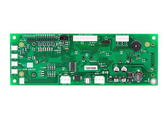


Just upload Gerber files, BOM files and design files, and the KINGFORD team will provide a complete quotation within 24h.