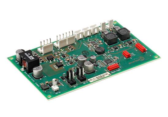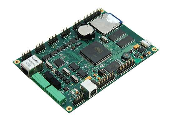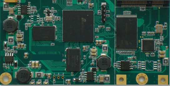
In PCBA processing, there may be a lot of small fragmentation problems, such as plating lamination and tin beads. Today, Shenzhen PCBA processing manufacturer -kingford will introduce the reasons for the formation of PCBA processing tin beads.
The cause of formation of tin beads in PCBA processing
1. When PCB board leaves liquid solder, it is very easy to form tin beads. This is because when the PCB board and tin wave are separated, they will pull into a tin column, but when the tin column breaks and falls back to the tin cylinder, it will sputter solder, solder falls on the PCB board to form tin beads. Therefore, in the design of tin wave generator and tin cylinder, attention should be paid to reduce the height of tin fall. A small drop height helps to reduce tin residue and spatter.
2. The second reason for the formation of tin beads is the release of gas from volatile substances in PCB board and solder resistance layer. If there are cracks in the metal layer of the PCB board through the hole, the heated gases of these substances will escape from the cracks and form tin beads on the component surface of the PCB board.
3. The third cause of tin bead formation has to do with flux. Flux can remain under components or between PCB boards and transporters (trays for selective welding). If the flux is not sufficiently preheated and burns out before the PCB board touches the tin wave, it will splash and form tin beads. Therefore, the flux supplier's recommended preheating parameters should be strictly followed.
This is the reason for the formation of PCBA processing tin beads, of course, there are many other small reasons can also cause the production of tin beads, but with the development of science and technology, technical personnel in the face of the production of tin beads also began to have rich experience, these experiences can also quickly help technical personnel to find solutions, this may be the charm of science and knowledge.

2. How to make PCBA test rack?
The PCBA test rack is a custom test device for testing PCBA finished products. When making PCBA test stands, PCBA processing plants usually need to provide Gerber files and PCBA samples to facilitate the production of test stands. Next, I will introduce the production steps of PCBA test stand.
PCBA test rack fabrication steps
1, material preparation
After determining the plan according to the data, it is necessary to prepare hardware materials (electronic components), related additional peripheral circuits, equipment, frame materials (such as acrylic board), glue, electrical batch, screws, wire materials, etc., to make the plan to determine the data.
2, the structure of the test frame to determine and check.
Three, wiring requirements
1. The opening port needs to be opened within 2mm, and the opening port of the wire and the tin line of the test needle should be tinned first.
2, the welded wire can not swing and loose phenomenon.
3. The strong and weak wires in the test frame are sorted out separately and bundled with wire.
4, ammeter and voltmeter joint must choose multimeter pen installation, can not install banana plug test current voltage and other functions, to ensure the safety of the operator.
5. The signal line of the high frequency product models must be grounded safely with the shielded wire.
6. The shell of the fire bull must be grounded within the measuring frame.
7, the test stand should be installed with fuse, can not be replaced with wire or other wires, the original plug on the 13A fuse removed, replace the fuse should pay attention to the test model needs much current, the replacement principle by the product working current 8-10 times.
4. Quality detection of selected points
The selection must follow the principle of comprehensive, effective and economical.
Use of PCBA test rack
PCBA test stand is widely used in the whole process of PCBA manufacturing, mainly used to test PCBA board after SMT patch and DIP plug-in. ICT test is mainly used, that is, to test the electrical conductivity of PCB board through test points, so as to determine whether the whole PCB board is successfully welded. The PCBA test rack is the main tool to assist this test.
The quality of PCBA test stand is related to the efficiency and pass-through rate of ICT test. Due to its long-term and frequent operation, it has a high requirement for its production quality, which requires sufficient attention from PCBA manufacturers.
Why do you choose kingford for PCBA processing?
1. Strength guarantee
▪SMT workshop: We have imported SMT machines and several sets of optical inspection equipment, with a daily output of 4 million. Each process is equipped with QC personnel, who can keep an eye on product quality.
▪DIP production line: We have two wave-soldering machines, among which there are more than 10 old employees who have worked for more than three years. The skilled workers can weld all kinds of plug-in materials.
2. Quality assurance, cost-effective
▪ High-end equipment can stick precision shaped parts, BGA, QFN, 0201 materials. Can also template patch, loose material hand.
▪ Sample and size batch can be produced, proofing from 800 yuan, batch 0.008 yuan/point, no start-up fee.
3. Rich experience in SMT and welding of electronic products, stable delivery
▪ Accumulated SMT SMT processing services for thousands of electronic enterprises, involving many kinds of automotive equipment and industrial control motherboard. The products are often exported to Europe and the United States, and the quality can be affirmed by new and old customers.
▪ On time delivery, normal 3-5 days after complete materials, small batch can also be expedited on the same day shipment.
4. Strong maintenance ability and perfect after-sales service
▪ Experienced maintenance engineers can repair all kinds of patch welding caused by bad products, to ensure the connection rate of each piece of circuit board.
▪ 24-hour customer service staff at any time response, the fastest speed to solve your order problems.


