
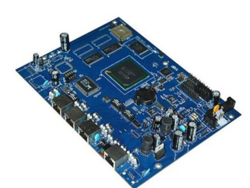
Professional PCB manufacturing and assembly
Building 6, Zone 3, Yuekang Road,Bao'an District, Shenzhen, China
+86-13410863085Mon.-Sat.08:00-20:00

SMT (Surface Mount Technology) is an important part of advanced manufacturing technology of modern electronic products. Its technical content includes surface assembly components, assembly substrate, assembly materials, assembly process, assembly design, assembly testing and detection technology, assembly and its testing and detection equipment, assembly system control and management, etc. The technical scope involves materials, manufacturing, electronic technology, detection and control, system engineering and many other disciplines, which is a comprehensive engineering science and technology.
SMT SMT technology main content:
The main content of surface assembly technology (hereinafter referred to as SMT technology) can be divided into four parts: assembly material selection, assembly process design, assembly technology and assembly equipment application.
SMT process technology involves chemical and material technology (such as various solder paste, flux, cleaning agent), coating technology (such as welding, printing), precision machining technology (such as screen making), automatic control technology (such as equipment and production line control), welding technology and testing, inspection technology, assembly equipment principle and application technology and many other technologies. It is the core of SMT and has the characteristics of SMT comprehensive engineering technology.
Design a structure size, terminal form, welding heat resistance
Surface assembly components - Manufacturing - manufacturing techniques for various components
Packing - braided tape, rod, pallet, bulk, etc
Electric subgrade board - single (multi) layer printed circuit board, ceramic, porcelain glaze metal plate, sandwich plate, etc
Assembly design - electrical design, thermal design, component layout, graphic wiring design of the substrate, etc
Friction materials - adhesive, solder, flux, cleaning agent, etc
Assembly process design - assembly mode, assembly process flow, process optimization design, etc
Assembly technology - coating technology, mounting technology, welding technology, cleaning technology, testing technology, etc
Application of assembly equipment - coating equipment, adhesive machine, welding machine, cleaning machine, test equipment, etc
Assembly system control and management -- assembly line or system composition, control and management, etc

2. What are the factors that affect the welding quality of BGA?
Nowadays, BGA (ball grid array) packaging technology is more and more used in electronic products, has become a common form of IC chip packaging. Large industrial control products, computer motherboards, small toys, wearable devices, are all inlaid with the figure of BGA.
BGA can be widely used in electronic products due to its advantages of small size, light weight and high performance. However, once the BGA is not welded properly during the SMT patch assembly process, it will seriously affect the quality of electronic products, and even lead to scrap.
Therefore, it is necessary for us to fully understand the factors affecting the quality of BGA welding, so as to optimize the SMT patch processing process, improve the quality of BGA welding, and ultimately improve the reliability of electronic products.
BGA welding principle
BGA is connected to the circuit board through the bottom solder ball, which can greatly improve the I/O number of the device, is conducive to shorten the signal transmission path, good heat dissipation performance. Moreover, due to the shorter lead length, the frequency characteristics are also effectively improved.
The BGA mounting process mainly includes the following steps:
Step 1 Bake
Not all BGA devices need to be baked. You should first determine if you need to bake according to the BGA package instructions. Most BGA are humidity sensitive components, and the package often contains humidity sensitive indicator cards. The color-changing humidity sensitive components will instruct the operator to bake the BGA components moderately to ensure their welding quality.
2. Solder paste printing
After the BGA is ready, the solder paste is printed on the BGA pad on the PCB by the solder paste press. The solder paste printing quality can be tested by SPI.
3. Patch
The BGA device is mounted through a vacuum nozzle, so that the bottom of the BGA device is completely coincident with the PCB pad.
4. Reflow welding
The solder ball of BGA, whose composition is usually 63Sn and 37Pb, has a melting temperature of about 183℃ and a diameter of 0.75mm. After high temperature reflow welding, the height of the solder ball will be reduced to 0.41mm to 0.46mm. After the temperature is cooled, the BGA device is firmly fixed on the PCB pad.
Step 5 Check
Due to the particularity of BGA structure, it is not possible to directly use the naked eye for welding inspection, but can only use AOI and X-ray detection to determine whether there are defects such as bridge, welding cavity and cold welding.
Factors affecting BGA welding quality
• PCB design
Because the circuit board is formed by the development and exposure process, it is almost impossible for all the lines to be evenly distributed, which results in different positions of the copper content on the circuit board. The subsequent result is that different areas of the printed circuit board have different heat absorption capabilities, and the areas with dense lines naturally absorb more heat. Therefore, when designing a PCB, BGA should not be placed in areas of high density wiring, or around larger copper pieces, or in areas with cuts or PCB diagonals.
• PCB quality
There are many factors affecting PCB quality. It can be said that the production quality of each link of PCB has direct or indirect influence on the reliability of PCB board. However, the main factor affecting the quality of BGA welding is ink treatment. BGA pad around the ink must be evenly distributed, otherwise it will lead to circuit or solder short circuit, and uneven ink will lead to bad through hole plug hole, therefore, to ensure the quality of BGA welding, must purchase high quality PCB circuit board.
• BGA devices
The packaging and storage of BGA components play a key role in the welding quality of BGA. BGA devices should be packed in vacuum to avoid oxidation of the welding ball of BGA devices and moisture. The oxidation of the welding ball and the dampness of the device usually lead to the deformation of the device in the high temperature environment, resulting in poor welding of the BGA device. The temperature and humidity of BGA devices should also be strictly controlled in storage to prevent the devices from getting damp and avoid poor welding.
• Process technology
BGA welding quality is closely related to patch technology, solder paste printing is the technical basis of patch processing. Therefore, high quality solder paste printing is conducive to the smooth completion of patch processing. The problems faced by solder paste printing, such as insufficient thickness, tip pulling and printing leakage, will cause poor BGA welding. In addition, technical control during the patch process is particularly important to avoid defects such as device offset, polarity reversal or clamping.


Just upload Gerber files, BOM files and design files, and the KINGFORD team will provide a complete quotation within 24h.