
Professional PCB manufacturing and assembly
Building 6, Zone 3, Yuekang Road,Bao'an District, Shenzhen, China
+86-13410863085Mon.-Sat.08:00-20:00

In the SMTprocess of the circuit board manufacturer, solder paste printing, the operation of the SMT machine and the welding of the reflow welding furnace should be listed as the key processes, so we first described from the inspection of the incoming materials in the SMT process.
Pre-assembly inspection (incoming inspection)
1. Inspection method
The main test methods include visual test, automatic optical test (AOI), X-ray test and ultrasonic test, online test, functional test and so on.
(1) Visual inspection refers to the method of inspecting assembly quality directly with the naked eye or with magnifying glass, microscope and other tools.
(2) Automatic optical inspection (AOI), mainly used for process inspection: solder paste printing quality inspection after printing press, paste quality inspection after mounting and post-welding inspection after reflow welding furnace. Automatic optical inspection is used to replace visual inspection: X-ray inspection and ultrasonic inspection are mainly used for welding spot inspection of BGA, CSP and Flip Chip.
(3) Online testing equipment using special isolation technology can test the resistance value of the resistor, capacitor capacitance value, inductor inductance value, polarity of the device, and short circuit (bridge), open (open) parameters, automatic diagnosis of errors and faults, and errors and faults display, print out.
(4) Function test for electrical function test and inspection of surface assembly plate. Functional measurement is to assemble the surface of a plate or table. The unit under test on the surface assembly board input electrical signals as a functional body, and then detect the output signals according to the design requirements of the functional body. Most functional tests have diagnostic procedures that can identify and determine faults. But function test equipment price is more expensive. The simplest functional test is to connect the surface assembly plate to the corresponding circuit of the equipment for power up to see whether the equipment can operate normally. This method is simple and less investment, but it can not automatically diagnose the fault.
The specific method used should be determined according to the specific conditions of each unit SMT line and the assembly density of the surface assembly board.
2. Incoming material inspection
Incoming material inspection is the primary condition to ensure the quality of surface assembly. The quality of components, circuit boards and surface assembly materials directly affects the assembly quality of surface assembly board. Therefore, the electrical performance parameters of components and weldability of welding ends and pins; Producible design of printed circuit boards and weldability of pads; The quality of surface assembly materials such as welding paste, patch adhesive, rod solder, flux and cleaning agent should have strict incoming inspection and management system.
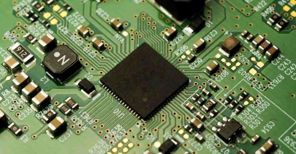
3. Surface assembly components (SMC/SMD) inspection
Main testing items of components: weldability, pin coplanar and serviceability, which should be sampled by the inspection department. The solderability of components can be tested by holding the body of components with stainless steel tweezers and dipping them into a tin pot at 235℃±5℃ or 230℃±5℃, taking them out at 2 soil 0.2s or 3 0.5s, and checking the solder end under a microscope at 20 times. Solder ends of components are required to be 90% tin. As a processing workshop, the following appearance inspection can be done:
(1) Visually or with a magnifying glass, check whether the welding end or pin surface of the components is oxidized and whether there are pollutants.
(2) The nominal values, specifications, models, accuracy and dimensions of the components shall be in accordance with the technical requirements of the products.
(3) The pins of SOT and SOIC cannot be deformed. For the multi-lead device QFP whose lead spacing is less than 0.65mm, the coplanicity of the pins should be less than 0.1mm (which can be detected by the optical mounting device).
(4) For products to be cleaned, the marks of components shall not fall off after cleaning, and the performance and reliability of components shall not be affected (visual inspection after cleaning).
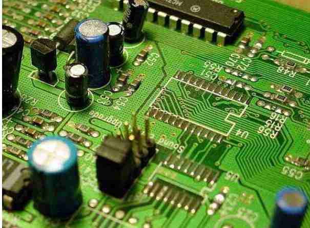
4. Printed circuit board (PCB) inspection
(1) PCB solder pad graphics and dimensions, solder resistance film, screen, through hole Settings should meet the design requirements of SMT printed circuit board. (For example: check whether the welding distance is reasonable, whether the screen is printed on the pad, whether the passthrough hole is done on the pad, etc.).
(2) The overall size of PCB should be consistent, and the overall size, positioning hole and reference mark of PCB should meet the requirements of production line equipment.
(3) Permissible warping size of PCB:
① Upward/convex: a maximum length of 0.2mm/5Omm a maximum length of 0.5mm/ the whole PCB length direction.
② Downward/concave: a maximum length of 0.2mm/5Omm a maximum length of 1.5mm/ the whole PCB length direction.
(4) Check whether the PCB circuit board is contaminated or damp


Just upload Gerber files, BOM files and design files, and the KINGFORD team will provide a complete quotation within 24h.