
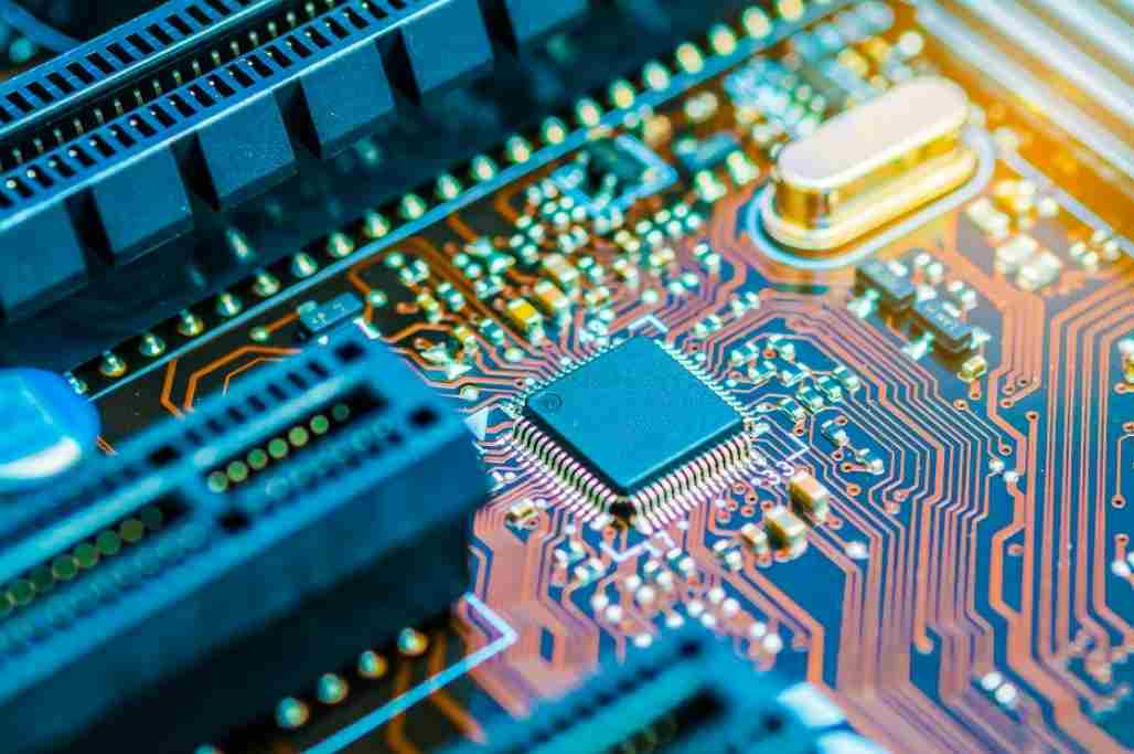
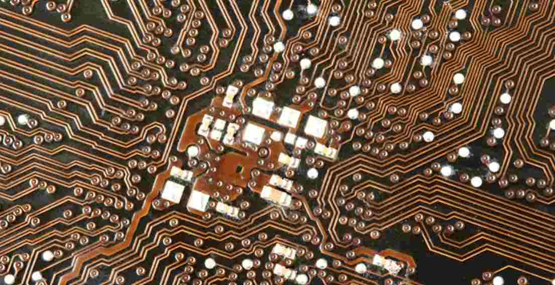
Professional PCB manufacturing and assembly
Building 6, Zone 3, Yuekang Road,Bao'an District, Shenzhen, China
+86-13410863085Mon.-Sat.08:00-20:00

The milling technology of circuit board CNC milling machine includes the selection of cutting direction, compensation method, positioning method, frame structure, the next cutter point, which is an important aspect to ensure the milling precision.
Cutting direction and compensation method:
When the cutter is cut into the plate, one of the cut faces is always facing the cutter's cutting edge, and the other is always against the cutter's cutting edge. The former is smooth and clean, with high dimensional accuracy. The main axis always turns clockwise. So whether the spindle fixed table movement or the table fixed spindle movement of the CNC milling machine, in milling printed PCB board external profile, to use counterclockwise direction of the knife.
This is commonly referred to as the inverse milling. And in the circuit board inside the milling frame or groove using the up-milling mode. Milling plate compensation is in milling plate machine automatically according to the set value so that the milling cutter automatically to the center offset of the milling line set half of the milling cutter diameter, that is, the radius distance, so that the shape of the milling and the program to keep consistent. At the same time, if the machine tool has the function of compensation must pay attention to the direction of compensation and the use of the program command, such as the use of compensation command error will make the appearance of the circuit board more or less equivalent to the length and width of the diameter of the milling cutter size.
Positioning method and cutting point:
Positioning methods can be divided into two kinds; One is internal positioning, and the other is external positioning. Positioning is also very important for process makers, generally in the pre-production of the circuit board should determine the positioning scheme.
Internal positioning is the universal method. The so-called internal positioning is the selection of printed PCB circuit board inside the installation hole, plugging hole or other non-metallic holes as positioning holes. The relative position of the hole should be on the diagonal and the hole of large diameter should be selected as far as possible. Do not use metallized holes. Because the difference in the thickness of the coating in the hole will affect the consistency of the hole you selected, and it is easy to cause damage to the coating in the hole and the edge of the hole surface when taking the board, the fewer the number of pins under the condition of ensuring the positioning of the printed circuit board, the better.
Generally small board using 2 pins, large board using 3 pins, its advantages are accurate positioning, PCB board shape deformation small precision high shape good, milling speed. The disadvantages of various aperture types in the plate need to prepare a variety of diameters of pins, such as there is no available positioning hole in the plate, in the early production need to discuss with the customer in the plate to add positioning holes, more cumbersome. At the same time each kind of board milling plate template different management is more troublesome, the cost is higher.
External positioning is another positioning method, is to add positioning holes on the outside of the board as the positioning hole of the milling board. Its advantage is easy to manage, if the production specification is good, milling plate template in general about 15. Because of the use of external positioning so can not be a board milling down, otherwise the circuit board is very easy to damage, especially the board, because the milling cutter and suction device will bring the board out of the circuit board damage and milling cutter break.
When the milling is finished, the program is paused and then the board is fixed with tape. The second section of the program is executed and the joint is drilled away with a 3mm to 4mm drill bit. Its advantage is that the template is small cost and easy to manage, can be milling all boards without installation holes and positioning holes of the circuit board, small process personnel management is convenient, especially CAM and other early production personnel production can be simplified, at the same time can optimize the utilization rate of substrate. Disadvantages are that the appearance of printed circuit board with at least 2-3 convex points is not beautiful because of the use of drill, which may not meet customer requirements, long milling time, and the labor intensity of workers is slightly larger.
Frame and lower cutting point:
Frame production is the production of the circuit board, frame design not only has an impact on the uniformity of electroplating, but also has an impact on the milling board, such as the design is not good frame easy deformation or in the milling board generated part of the small block of small waste block, the waste block will block the suction pipe or break the high-speed rotation of the milling cutter, frame deformation, especially when the external positioning of the milling board caused by the finished board deformation, In addition, the tool point and machining sequence is selected well, which can make the frame maintain the maximum strength and the fastest speed. The choice is not good, the frame is easy to deform and make the printed board scrap.


Just upload Gerber files, BOM files and design files, and the KINGFORD team will provide a complete quotation within 24h.