
Professional PCB manufacturing and assembly
Building 6, Zone 3, Yuekang Road,Bao'an District, Shenzhen, China
+86-13410863085Mon.-Sat.08:00-20:00

The 1.20H principle refers to the 20H distance between the power layer and the formation, which is also to suppress the edge radiation effect. The edge of the plate radiates electromagnetic interference. The power layer is shrunk so that the electric field is conducted only within the range of the ground. Effectively improve EMC. If the retraction is 20H, 70% of the electric field can be limited within the grounding edge. The retraction of 100H can contain 98% of the electric field.
The 20H rule is used to ensure that the edge of the power plane is retracted at least 20 times more than the edge of the 0V plane. This rule is often required as a technique for reducing side-shot emission from 0V/ power plane structures (suppressing edge radiation effects).
However, the 20H rule provides significant benefits only under certain conditions. These specific conditions include: 1. The rise/fall time of current fluctuation in the power bus is less than 1 NS.
2. The power plane shall be located on the internal level of the PCB, and the upper and lower levels adjacent to it are 0V planes. The two 0V planes should extend outward at least 20 times as far apart as the layers between them and the power plane.
3. The power bus structure does not generate resonance at any frequency of concern.
4. The total derivative of PCB board should be at least 8 layers or more
2. How to place and install the decoupling capacitor
The size of the digital circuit output current Ioh pulled from the power supply at high voltages and the current Iol injected at low voltages is generally different, namely: Iol> Ioh. TTL and non gates in the following figure illustrate the formation of the spike current:
The theoretical waveform of the supply current shows a short but large spike in the supply current when the output changes from low level to high level. The waveform of the peak supply current varies with the type of device used and the capacitance load attached to the output.
The main causes of the spike current are:
Output stage T3, T4 tube short design at the same time conduction. In the process of switching from the output low level to the high level at the and non gate, the negative jump of the input voltage generates a large reverse drive current in the base loops of T2 and T3. Since the saturation depth of T3 is designed to be larger than that of T2, the reverse drive current will make T2 first break away from saturation and cut off. After T2 cutoff, its collector potential rises and T4 is switched on. But T3 is not out of saturation at this time, so in the very short design T3 and T4 will be switched on at the same time, resulting in a large ic4, so that the supply current into a peak current.
Low power TTL gate R4 is larger, so its peak current is smaller. When the input voltage changes from low level to high level and the output level of non-gate changes from high level to low, T3 and T4 may also be switched on at the same time. However, when T3 begins to enter the conduction, T4 is in the amplified state, and the collection-emission voltage between the two tubes is large, so the peak current generated is small and the influence on the power supply current is relatively small.
Another reason for spiking current is the effect of load capacitance. There is actually a load capacitor CL at the output end of the non-gate. When the output of the gate is converted from low to high, the supply voltage is charged by T4 to the capacitor CL, thus forming a peak current.
When the output of the and non gate is converted from a high level to a low level, the capacitor CL is discharged through T3. In this case, the discharge current does not pass through the power supply, so the discharge current of CL has no influence on the power supply current.
The suppression method of peak current:
1. Take measures on the circuit board wiring to minimize the stray capacitance of the signal line;
2, the other way is to try to reduce the internal resistance of the power supply, so that the peak current will not cause too much power supply voltage fluctuation;
3, the usual method is to use decoupling capacitor to filter, generally in the circuit board at the power entrance
A 1uF ~ 10uF decoupling capacitor filters out low frequency noise; A 0.01uF ~ 0.1uF decoupling capacitor (high frequency filter capacitor) is placed between the power supply and ground of each active device in the circuit board to filter out high frequency noise. The purpose of filtering is to filter out the AC interference superimposed on the power supply, but it is not always better to use the larger capacity of the capacitor, because the actual capacitor is not an ideal capacitor and does not have all the characteristics of the ideal capacitor.
The selection of decoupling capacitance can be calculated as C=1/F, where F is the circuit frequency, that is, 10MHz is 0.1uF, 100MHz is 0.01uF. Generally, 0.1-0.01uF can be used.
The high frequency filter capacitor placed near the active device has two functions: one is to filter out the high frequency interference transmitted along the power supply, the other is to timely supplement the peak current required when the device works at high speed. So the position of the capacitor needs to be considered.
Due to the existence of parasitic parameters, the actual capacitor can be equivalent to the resistance and inductance in series on the capacitor, which are called equivalent series resistance (ESR) and equivalent series inductance (ESL). In this way, the actual capacitor is a series resonant circuit, whose resonant frequency is:
How to place and install decoupling capacitors in PCB layout
The actual capacitance is capacitive at frequencies below Fr and inductive at frequencies above Fr, so the capacitance is more like a band-stop filter.
Due to its large ESL and Fr less than 1MHz, 10uF electrolytic capacitor has a good filtering effect on 50Hz low-frequency noise, but has no effect on hundreds of megabits of high-frequency switching noise.
The ESR and ESL of a capacitor are determined by the structure of the capacitor and the medium used, not the capacitance. The ability to suppress high-frequency interference is not improved by using larger capacitors. Capacitors of the same type have less impedance than smaller capacitors at frequencies lower than Fr, but if the frequency is higher than Fr, the ESL determines that there is no difference in impedance between the two.
Using too many large capacity capacitors on the board is not helpful in filtering out high-frequency interference, especially when powered by a high-frequency switching power supply. Another problem is that too many large-capacity capacitors increase the impact on the power supply when powering on and hot-swapping the circuit board, which is easy to cause problems such as power supply voltage drop, circuit board connectors spark, circuit board voltage rise slowly and so on.
The decoupling capacitor is placed in PCB layout
For capacitor installation, the first thing to mention is the installation distance. The capacitor with the smallest capacity has the highest resonant frequency and the smallest decoupling radius, and is therefore placed closest to the chip. Larger capacity can be a little farther away, the outermost place the maximum capacity. However, all capacitors decoupled from the chip are kept as close to the chip as possible
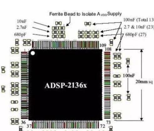
Here is an example of placement. The capacitance levels in this example roughly follow the 10-fold class relationship.

How to place and install decoupling capacitors in PCB layout
Another point to note is that when placed, it is best to distribute evenly around the chip for each capacity level. Usually the design of the chip takes into account the arrangement of power and ground pins, which are generally evenly distributed on the four sides of the chip. Thus, voltage perturbations exist on all sides of the chip, and decoupling must also be evenly decoupled across the entire chip region. If you put all the 680pF capacitors in the figure above on the upper part of the chip, you will not be able to decouple the voltage perturbations in the lower part of the chip well because of the decoupling radius problem.
Installation of capacitance
To install the capacitor, pull a short lead wire from the pad and connect it to the power plane through the hole, as well as the ground end. In this way, the current loop through the capacitor is: power plane - "through the hole -" lead wire - "pad -" capacitor - "pad -" lead wire - "through the hole -" ground plane,
How to place and install decoupling capacitors in PCB layout
The first method leads a long lead wire from the pad and connects it through the hole. This introduces a large parasitic inductance. It must be avoided.
The second method is to drill holes in the two ends of the pad next to the pad, which is much smaller than the first method, and the parasitic inductance is also smaller, which is acceptable.
The third in the side of the pad drilling, further reduce the loop area, parasitic inductance is smaller than the second, is a better method.
The fourth is drilled on both sides of the pad. Compared with the third method, each end of the capacitor is connected to the power plane and ground plane in parallel through the hole, which is smaller than the third parasitic inductance. As long as the space allows, try to use this method.
The last method is to punch holes directly on the pad, the parasitic inductance is minimal, but welding is likely to cause problems, whether to use depends on the processing capacity and way.
The third and fourth methods are recommended.
It is important to note that some engineers, in order to save space, sometimes have multiple capacitors use common through-holes. Do not do this under any circumstances. It is best to find ways to optimize the design of the capacitor combination and reduce the number of capacitors.
Because the wider the printed line, the smaller the inductance, from the pad to the hole lead as wide as possible, and if possible, try to be the same width as the pad. This allows you to use 20mil wide leads even for 0402 capacitors.


Just upload Gerber files, BOM files and design files, and the KINGFORD team will provide a complete quotation within 24h.