
Professional PCB manufacturing and assembly
Building 6, Zone 3, Yuekang Road,Bao'an District, Shenzhen, China
+86-13410863085Mon.-Sat.08:00-20:00

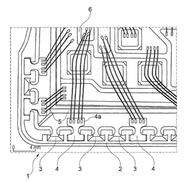
1.SMT reflow welding requires that the pads of the two end Chip components should be independent pads. When the pad is connected with a large area of ground wire, the cross paving method and 45° paving method should be preferred; The length of the conductor leading from the ground or power cord with a large area is 0.5mm and the width is less than 0.4mm; The wire connected with the rectangular pad should be led from the center of the long side of the pad to avoid a certain Angle. See Figure (a) for details.

See Figure (b) for the wires between SMD pads and the lead wires from the pads. The diagram shows the connection diagram of pad and printed wire.
PCB routing design printed conductor direction and shape
(1) The printed wire of the PCB in SMT should be very short. Therefore, if you can go the shortest, do not go complicated. Follow the easy, not complicated, not short, not long. It is of great help to the quality control of PCB circuit board in the later stage.
(2) The direction of the printed wire shall not have sharp bending and acute Angle, and the Angle of the printed wire shall not be less than 90°. This is because it is difficult to corrode the smaller inner corners when making the board. Copper foil is easily stripped or warped at outer corners that are too sharp. The best form of turning is gentle transition, that is, the inside and outside Angle of the corner is the best radian.
(3) When the wire passes between two gaskets but is not connected with them, it shall maintain a maximum and equal distance from them; Similarly, the distance between wires should be uniform and equal, and maintained at maximum.
(4) When connecting wires between PCB pads, when the center distance between the pads is less than the outer diameter of the pads D, the width of the wires can be the same as the diameter of the pads; When the center distance between pads is greater than D, the width of the wire should be reduced. When there are more than 3 pads on the pad, the distance between the wires should be greater than 2D.
(5) Copper foil should be reserved for common ground wires as far as possible.
(6) In order to increase the peeling strength of the gasket, a production line without electrical conductivity can be provided. PCB circuit board
When many customers make products for the first time, he is not very familiar with them. When he comes, he asks you if this is Shenzhen kingford Co., LTD. I have pictures of this board, always say that you according to my in accordance with my photos do exactly the same, but in fact PCB design is a very complex knowledge, welding pad, wire, wiring these.
2.SMT patch processing template manufacturing process requirements
1. What are Mark's processing procedure specifications?
1. The processing method of Mark, whether Mark is needed, which side of the template, etc.
2. Which side of the Mark graphic should be placed on the template should be determined according to the specific structure of the printing press (camera position).
3, Mark point cutting depends on the printing press, there are printing surface, non-printing surface, two sides of the half cut, full cut vinyl and so on.
Two, whether the board, and the requirements of the board. If the board is assembled, the PCB file of the board should be given.
Three, insert the welding disc ring requirements. Because the reflow welding process of plug-in components requires more welding paste than that of mounted components, special requirements can be put forward if some plug-in components need to adopt the reflow welding process.
Four, the template (pad) opening size and shape modification requirements. Usually greater than 3mm of the pad, in order to prevent the pattern of the solder paste from falling back and prevent tin beads, the opening uses the way of "bridge", the line width is 0.4mm, so that the opening is less than 3mm, can be evenly divided according to the size of the pad. Various components on the template thickness and opening size requirements.
1, μBGA/CSP, Flip Chip with square opening than circular opening printing quality.
2. When using no cleaning solder paste and using no cleaning process, the opening size of the template should be reduced by 5% ~ 10% :
3. The opening design of the lead-free process template is larger than that of the lead, and the solder paste is completely covered with the pad as far as possible.
4. Proper opening shape can improve SMT patch processing effect. For example, when the Chip component size is less than metric 1005, the solder paste on both ends of the pad is easily adhered to the bottom of the component due to the small distance between the pads, and it is easy to create a bridge and solder ball at the bottom of the component after flow welding. Therefore, when processing templates, the inner side of a pair of rectangular pad openings can be modified into a sharp Angle or bow shape to reduce the amount of solder paste at the bottom of the components, which can improve the bonding sound at the bottom of the components, as shown in the figure. The specific modification scheme can be determined by referring to the "welding paste template Opening Design" data in the template processing factory.
V. Other requirements
1. According to the PCB design requirements, ask whether the test point needs to open or not. If there is no special explanation for the test point, do not open.
2. Whether there are electric polishing process requirements. Electropolishing is used for formwork with openings less than 0.5mm apart.
3, use (explain the processing template for printing solder paste or printing patch glue).
4. Whether the template needs to be engraved with characters (PCB product code, template thickness, processing date and other information can be engraved without penetration).
Vi. After receiving the Emil and fax, the template factory shall send back the "Demander confirmation" fax according to the Demander's request.
1. If there is any problem, contact us by telephone or fax, and we can process it after the customer's confirmation.
2. Check whether the size of the mesh frame meets the requirements, place the template flat on the table, press the surface of the stainless steel mesh plate by hand, and check the tension
Net quality, the tighter the net, the better the printing quality. In addition, should also check the mesh frame around the bond quality
3. Lift the template for optical inspection, check the appearance quality of the template opening, and check whether there are obvious defects, such as the shape of the opening and whether the distance between the IC pin adjacent openings is abnormal.
4. Use a magnifying glass or microscope to check whether the horn of the welding disc opening is down, whether the inner wall around the opening is smooth and whether there is burr, and focus on checking the processing quality of the narrow spacing IC pin opening.
5. Put the printed board of the product under the template, align the leaking hole of the template with the printed board solder plate figure, and check whether the figure is complete
Full alignment, no porosity (unnecessary openings) and few holes (floor drain openings).
6. If the problem is found, it should first check whether it is our confirmation error, and then check whether it is processing problem. If quality problem is found, it should feedback to the template PCB manufacturing factory and negotiate to solve it.


Just upload Gerber files, BOM files and design files, and the KINGFORD team will provide a complete quotation within 24h.