
Professional PCB manufacturing and assembly
Building 6, Zone 3, Yuekang Road,Bao'an District, Shenzhen, China
+86-13410863085Mon.-Sat.08:00-20:00

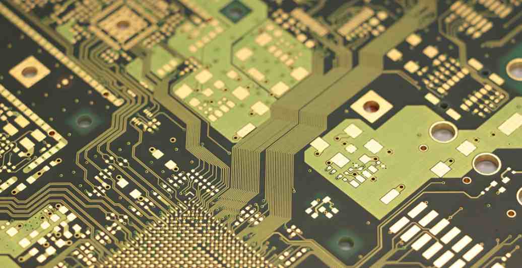
When we finish the design of PCB board, need to choose the circuit board surface treatment process, now commonly used circuit board surface treatment process has HASL (surface spray tin process), ENIG (gold sinking process), OSP (oxidation prevention process), commonly used surface treatment process we how to choose? Different PCB surface treatment processes, charges are different, the final effect is different, you can choose according to the actual situation, I will tell you the advantages and disadvantages of HASL, ENIG, OSP these three different surface treatment processes.
1. HASL (surface tin-spraying process)
Tin spraying process is divided into lead and lead-free tin spraying process, tin spraying process used to be the most important surface treatment process in the 1980s, but now, less and less circuit boards choose tin spraying process, the reason is that the circuit board toward the "small and fine" direction of development, tin spraying process will lead to fine components welding will have tin beads, spherical tin point caused by poor production, In order to pursue higher process standards and production quality, PCBA processing plants often choose ENIG and SOP surface treatment processes.
Advantages of lead spray tin: lower price, excellent welding performance, mechanical strength, gloss than lead spray tin.
Disadvantages of lead spray tin: lead spray tin contains lead heavy metals, production is not environmental protection, can not pass ROHS and other environmental protection evaluation.
Advantages: Low price, excellent welding performance, and relatively environmental protection, can pass ROHS and other environmental protection evaluation.
Lead-free spray tin disadvantages: mechanical strength, gloss, and so on as good as lead-free spray tin.
Common disadvantages of HASL: It is not suitable for welding fine clearance pins and small components because of the poor surface smoothness of the tinspray plate. Tin beads are easy to be produced in PCBA processing, which is easy to cause short circuit to pin components with fine clearance.
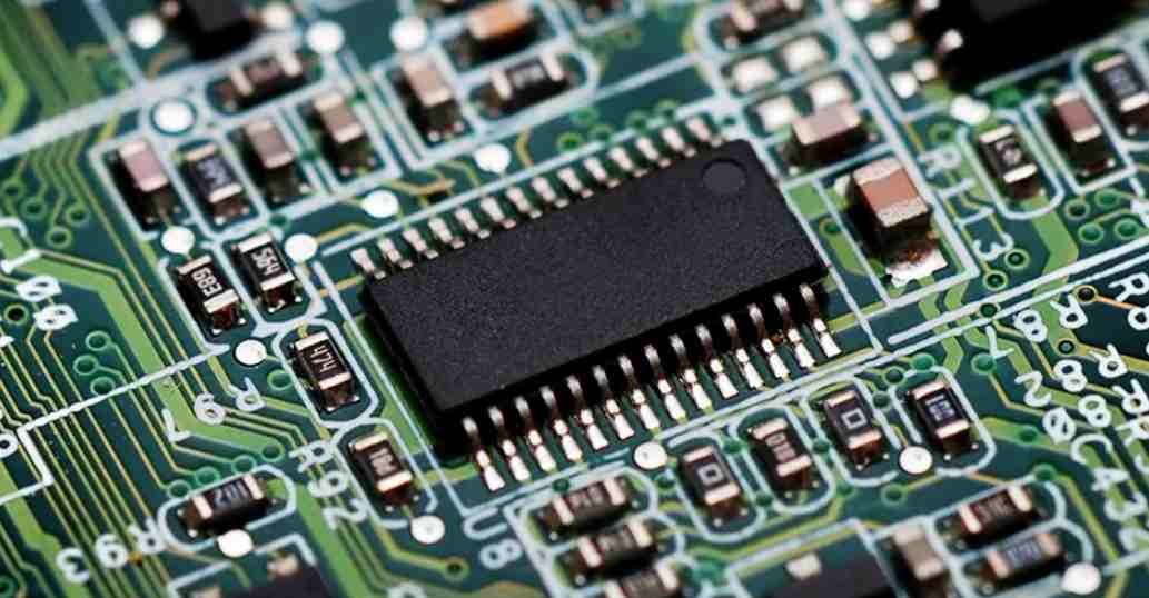
2. ENIG (Gold Sinking Process)
Gold sinking process is a relatively advanced surface treatment process, mainly used in the surface of the PCB circuit board with connection functional requirements and long storage life.
Advantages of ENIG: It is not easy to oxidized, can be stored for a long time, and the surface is flat. It is suitable for welding components with fine clearance pins and small solder joints. It can be repeated multiple times without much loss of weldability. Can be used as the base material for COB wire.
Disadvantages of ENIG: High cost, poor welding strength, because of the use of nickel-free plating process, prone to black disk problems. The nickel layer oxidizes over time, and long-term reliability is an issue.
3. OSP (anti-oxidation process)
OSP is the chemical formation of an organic skin film on the surface of bare copper. This layer of film has anti-oxidation, heat shock, moisture resistance, to protect the surface of copper in the normal environment no longer continue to rust (oxidation or vulcanization, etc.); Equivalent to an anti-oxidation treatment, but in the follow-up welding high temperature, the protective film must be easy to be quickly removed by the flux, the exposed clean copper surface can be immediately combined with the molten solder in a very short time to become a firm solder joint. The percentage of boards using the OSP surface treatment process has increased significantly, as this process is suitable for both low and high process boards. If there are no surface connection functional requirements or storage life limitations, OSP is the most desirable surface treatment process.
Advantages of OSPs: With all the advantages of bare copper plate welding, expired (three months) boards can also be resurfaced, but usually only once.
Disadvantages of OSPs: Easy to be affected by acid and humidity. When used for secondary reflow welding, it should be completed within a certain time, usually the second reflow welding effect will be poor. If it lasts longer than three months, it must be resurfaced. It should be used within 24 hours after unpacking. OSP is the insulating layer, so the test point must be printed with solder paste to remove the original OSP layer before it can contact the pin point for electrical testing. The assembly process requires major changes. If probing raw copper surfaces is detrimental to ICT, over-pointed ICT probes may damage the PCB, requiring manual preventive treatment, limiting ICT testing and reducing repeatability of testing.
The above is about HASL, ENIG, OSP circuit board surface treatment process analysis, you can choose which surface treatment process according to the actual use of the circuit board.
Process analysis of PCBA welding cooling
Feb 17,2023


Just upload Gerber files, BOM files and design files, and the KINGFORD team will provide a complete quotation within 24h.