
Professional PCB manufacturing and assembly
Building 6, Zone 3, Yuekang Road,Bao'an District, Shenzhen, China
+86-13410863085Mon.-Sat.08:00-20:00

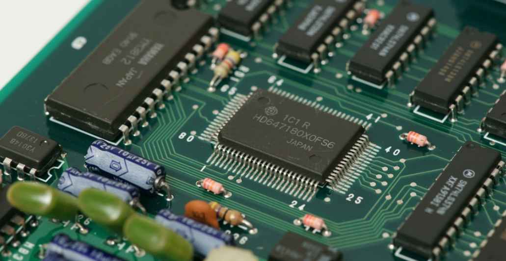
With the development of economy and science and technology, people put forward higher and higher requirements for electronic products with multi-function, miniaturization, high density, high performance and high quality. Therefore, for PCBA processing industry, high welding quality is the life insurance of electronic products.
Why SMT welding is one of the important links in the assembly process of electronic products. If there is no corresponding SMT welding process quality assurance, then any well-designed electronic equipment is difficult to achieve the design goal. Therefore, when welding to strictly check the solder joint, to prevent the appearance of unqualified solder joint quality problems resulting in unqualified electronic products. The following to introduce a variety of electronic SMT welding shortcomings.
After the SMT welding operation, the welding quality work shall be checked in order to make the product have reliable function. Welding inspection is generally for appearance inspection, not only to check the solder joint, but also to check the condition around the solder joint, such as because of the problems derived from welding. The inspection of wiring welding of terminal post is to check whether the insulation skin of the wire used is damaged or not from the welding condition, and whether the terminal post is scarred. The bending degree and tightness of the hook hook of the hook welding wire, whether there are dirty points in each part, etc. Many of the functional damage of electronic components found in the electrical function inspection is caused by poor welding.
After all, the welding of electronic products is mainly used for electrical connections. If the electrical connection has defects of the product presents a problem, must be repaired, eliminate its shortcomings.
However, in actual manufacturing, welding defects often occur, especially during the reflow phase. In fact, welding problems at this stage are not entirely caused by reflow technology, because SMT welding quality is closely related to the manufacturability of PCB pads, steel mesh design, weldability of components and PCB pads, manufacturing equipment status, and solder quality. Each link paste and technical parameters as well as each worker's operating skills.
There may be problems in every link, which will affect the quality of SMT welding. In this article, elements that may affect the quality of SMT welds are discussed and analyzed to avoid similar problems in actual manufacturing.
BOM preparation
As one of the most important composite materials in SMT, BOM quality and performance are directly related to the quality of reflow welding. Specifically, the following must be taken into account:
1. Component packaging must meet the automatic installation requirements of the installation regulations.
2, the parts graphics must meet the requirements of automatic SMT, because it must have a high dimensional accuracy of the standard shape.
3. The welding quality of the weldable end of the component and PCB pad shall meet the requirements of reflow welding, and the weldable end of the component and pad shall not be contaminated or oxidized. If the weldable ends of the components and PCB pads are subjected to oxidation, contamination or moisture, some welding defects may occur, such as poor wetting, pseudo-welds, welding beads or cavities. This is especially true for humidity sensors and PCB management. Humidity sensors must be vacuum-packed and stored in a drying oven, and it is necessary to bake them before the next manufacture.
Manufacturability design of PCB pad
The level of SMT depends on PCB design quality and is the first factor affecting surface mount quality. Based on statistics from HP, 70 to 80 percent of manufacturing defects from derived PCB design problems are in substrate material selection, conversion component layout, pad and thermal pad design, solder mask design, package type of components, component method, transmission boundary, through positioning, optical registration point, EMC (electromagnetic compatibility), etc.
For PCBS with the correct pad design, even if a little skew occurs during surface installation, it can be corrected under the action of the surface tension of molten tin, which is called automatic positioning or self-correcting effect. However, if the PCB pad is not designed correctly, welding defects such as component offset and stellings can still be encountered, even if the installation position is very accurate. Therefore, the following aspects must be carefully considered in the design of SMT pad.
1, the symmetry of the welding pad. To avoid position deviation and stalling problems after reflow soldering, for chip components 0805 and below, the pads at both ends should be symmetrical in terms of pad size and heat absorption and dissipation capacity to maintain a balance of melting surface tension. Solder. If one end is on a large copper foil, it is recommended to use a single wire connection to attach the pad on the large copper foil.
2. Space between pads. To ensure the proper size of the lap between the end of the assembly or the pin and the pad, welding defects often result when the space between the pad is too large or too small.
3. The remaining size of the pad must ensure the crescent-shaped weld point after the lap between the end of the assembly or the pin and the pad.
4. The width of the pad should be basically compatible with the width of the component end or pin.
5. Do not place through holes on the pad. Otherwise, molten tin may flow away along the through-hole during reflow soldering, resulting in pseudo-welding and tin deficiency. It can flow to the other side of the board and cause a short circuit.
Component installation
The quality of component installation depends on three factors: correct selection of components, accurate placement, and appropriate mounting pressure. The correct selection of components refers to the fact that the components must be compatible with the requirements of the BOM. Proper placement means that the coordinates must be installed correctly, and the accuracy of the installation procedures must ensure installation stability and proper installation of the components on the pad. At the same time, attention must be paid to the mounting Angle to ensure that the component is oriented correctly. Appropriate mounting pressure refers to the pressing thickness of the component and is never too small or too large. The mounting pressure can be determined by setting the PCB thickness, the component package thickness, the nozzle pressure of the mounter and adjusting the Z axis of the mounter.
Reflow welding
The welding quality of the solder joint depends on the correct setting of reflow temperature curve. A good reflow soldering curve requires that all mounting components on the PCB receive excellent soldering and that the soldering points should be of excellent appearance and high quality. If the temperature rises too fast, on the one hand, the component and PCB will be heated, so that the component is easy to damage and PCB deformation. On the other hand, the solvent in the solder paste evaporates too quickly, and the metal complex will splash out as a tin ball. The peak temperature is usually set to 30 ° C to 40 ° C above the melting point of the solder paste. If the temperature is too high and the reflux time is too long, it will damage the heat-resistant components or component plastics. In contrast, incomplete melting of the solder paste will result in a reliable solder spot. In order to improve welding quality and prevent component oxidation, nitrogen reflux welding can be applied. The reflux curve is usually set according to the following aspects:
(1) Can be set according to the recommended temperature curve of the solder paste. The composition of solder paste determines its activation temperature and melting point.
(2) According to the thermal performance parameters of heat-resistant components and valuable components, for some special components, the maximum welding temperature must be considered.
(3) It should be set according to the material, size, thickness and weight of PCB substrate.
(4) It should be set according to the structure of reflow furnace and the length of temperature zone, and different reflow furnace should have different Settings.
There are many factors affecting SMT welding quality, including component weldability, PCB quality, PCB pad design, solder paste quality, PCB manufacturing quality, SMT manufacturing equipment condition, SMT technical parameters of each link and the operating skills of each worker. Among these elements, the quality of the components, PCB and solder paste, as well as PCB design, are critical to reflow welding quality assurance because welding defects caused by these elements are difficult or impossible to solve through technical solutions. Therefore, the first condition to improve excellent welding quality is good control of material quality and excellent PCB pad design. In addition, solder paste printing process of each link of the technical parameters.
Solder paste printing
Feb 17,2023


Just upload Gerber files, BOM files and design files, and the KINGFORD team will provide a complete quotation within 24h.