
Professional PCB manufacturing and assembly
Building 6, Zone 3, Yuekang Road,Bao'an District, Shenzhen, China
+86-13410863085Mon.-Sat.08:00-20:00

Now officially cut into the process of making circuit boards. Some people will say, you are not to explain the circuit board preset, a preset, why to spend such a huge effort to Shaojie circuit board process?
This is because whether it is circuit presets or circuit board presets, it is in order to manufacture satisfactory circuit boards in the future, and successfully realize the value of its research and development and the target of mass production. If the production failure as a good opponent, then we should have a good understanding of our opponent.
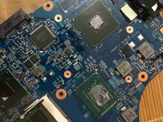
Manufacturing process of 4 - layer PCB circuit board
(1) Drawing film using Laser photo plotters(laser plotters), manufacturing wiring film, welding resistance layer film, printing film and other essential films in the production project. Film in the adhesion process, some will reveal a little error, especially for special plate, error will be a little larger. Therefore, in the circuit board preset to fully consider the problem to the impact of these errors, make appropriate preset.
(2) the cutting of the board to make the board of the circuit board in the factory size is generally 1m×1m or 1m×1.2m. According to the production needs to cut into a different volume of parts (work), according to the volume of their own preset PCB circuit board to select the given size of the parts, to prevent consumption, increase the indispensable cost.
(3) Forming of the inner circuit Next, the formation of the inner circuit wiring. The sensitive dry film is adhered to the double-sided copper plate as the inner layer, and then affixed to the film used to manufacture the inner layer of wiring, the exposure, and then the development treatment, leaving only the required place of wiring. This project should be implemented on both sides; it should remove unnecessary copper foil through Etching equipment.
(4) oxygen treatment (blackening treatment) before synthesis with the outer layer, copper foil should be oxygenated to form a small concave and convex appearance. This is to increase the size of the contact plane or surface between the semi-curing agent (prepreg), which has insulation and adhesion, and the inner layer, so that the adhesion is better. Now in order to mitigate background pollution, the development of oxygen treatment of the replacement, and now the circuit board itself has a good contact.
(5) Lamination treatment Lamination treatment, through the oxygen treatment of the inner circuit, covered with semi-curing agent, and then affixed with the outer copper plate. Under vacuum condition, while heating, through the laminating machine for compression. Semi-curing agent acts as adhesion and insulation. After the lamination disposal, and the exterior of the two-sided copper plate specially look the same, from this engineering and the two-sided copper plate engineering is the same.
(6) Hole digital control machine tool for hole operation.
(7) Removal of residue due to the initiation of calories when opening holes will cause supplement ablation, and attached to the inner wall of the electroplating hole, can be cleaned by chemical drugs, make the inner wall smooth and increase the reliability of copper plating.
(8) copper plating in the outer layer of co-signed needs to be disposed of by copper plating, the first is no electrolytic plating, the formation of the minimum thickness of the flow of current. Secondly, in order to achieve the preset required plating thickness, electrolytic plating treatment is implemented. Because the outer copper foil is also attached to the copper plating, the thickness of the outer wire is the thickness of the copper foil plus the plating thickness.
(9) the formation of the outer circuit and the formation of the inner circuit at the same time, stick to the dry film of respiratory tract infection light, and then close to the wiring film on the surface, the implementation of exposure, exposure phenomenon, leaving only the place where the line needs to go, both sides of the implementation of treatment, and then, after the corrosion treatment, do not remove the copper foil.
(10) Manufacturing solder resistance layer In order to form a pad, the need to implement solder resistance layer (insulation layer) forming treatment, but also in order to try to take care of the copper foil and better insulation. The method can be through the direct paste film, or is first coated with natural resin and then paste film, after exposure and development to get rid of unnecessary places.
(11) The appearance of the disposal of no solder resistance layer and exposed copper parts, in order to avoid oxygen, the need to implement lead, lead-free copper plating, electrolytic or non-electrolytic gold plating, or water-soluble chemical cleaning agent appearance disposal.
(12) The printing is generally white, and the solder resistance layer is green. For the LED lamp PCB board, in order to achieve a better consolidation of the light source effect, the printing is black, the welding resistance layer is white color. Or simply leave out the printing.
Printing can be used to install and check the numbering of electronic components. But for the sake of the secrecy of the circuit, sometimes the printing is sacrificed.
(13) Contour processing through counting numbers to control the punching machine or production model of the circuit board contour processing
(14) Electrical inspection and determination engineering through special electrical inspection and determination facilities, circuit board and short circuit inspection and determination
(15) Shipping check the appearance and number of circuit boards can be shipped, generally with deoxygenated materials for packaging, or directly to the installation of components of the factory.


Just upload Gerber files, BOM files and design files, and the KINGFORD team will provide a complete quotation within 24h.