
Professional PCB manufacturing and assembly
Building 6, Zone 3, Yuekang Road,Bao'an District, Shenzhen, China
+86-13410863085Mon.-Sat.08:00-20:00

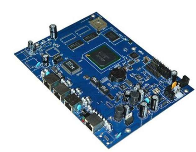
PCBA processing and production process often uses two types of test rack, one is pcb test rack, the other is PCBA test rack, often customers will confuse this kind, some customers will not know what these test rack is used for, the following by global Wei technology to introduce the principle and use of these two kinds of test rack.
Principle of the test stand: The principle of the PCB test stand and the PCBA test stand is very simple. Both of them are connected to the welding pad and the test point on the PCB board through the metal probe. When the PCB board is energized, the voltage value and the current value of the test circuit and other typical values and phenomena are obtained.
PCB test rack is customized according to customer requirements, according to the need to produce PCB board size, solder joint location to decide. It is mainly composed of epoxy plate, metal probe, wire and detection interface.
Mainly used for circuit board circuit breaker detection, never ensure that the product does not appear bad phenomenon, short circuit and open circuit and so on.
PCBA board test rack is dedicated to the board, according to the production of pcb board size test point position and a variety of external instrumentation, interface and accessory circuit board to compose, commonly used material is acrylic, bakbakary and so on to make the main body of the frame, match some contact with the thimble wire link, the shape of a simple test rack.
PCBA test stand is an indispensable test tool in SMT patch processing and production. It can mainly test the produced circuit board, and determine whether the board is a good product by the detected signals, pictures, sound temperature and so on.

2.Patch processing process
The production and processing of PCB OEM includes many kinds of processing technology, such as PCB manufacturing, SMT patch processing, DIP plug-in, test assembly, such as PCB manufacturing, SMT patch processing, dip plug-in, test Assembly, etc. PCBA patch processing technology plays an important role in the miniaturization and precision development of electronic products. kingfordPCBA OEM Pate Electronics will briefly introduce some patch processing process.
1. Solder paste printing: solder paste or patch glue is leaked onto the solder pad of PCBA to prepare for the welding of components.
Two, dispensing: the glue drops to the fixed position of the PCBA board, its main role is to fix the components to the PCB board. The glue drops to the fixed position of the PCBA board, its main role is to fix the components to the PCB board.
Iii. Patch: precise installation of surface assembly components to the fixed position of PCBA.
Four, curing: the patch adhesive ablation, so that the surface assembly components and PCB board solid bonding together.
Reflow welding: The surface assembly components are welded together with the PCBA plate.
6. Cleaning: Its function is to remove welding residues such as flux that are harmful to human health on the assembled PCBA.
Vii. Detection: It detects the welding stop quality and assembly quality of assembled PCBA.
Viii. Repair: Stop rework of PCBA board with defects detected.
Explain the process of PCB circuit board
Feb 15,2023


Just upload Gerber files, BOM files and design files, and the KINGFORD team will provide a complete quotation within 24h.