
Professional PCB manufacturing and assembly
Building 6, Zone 3, Yuekang Road,Bao'an District, Shenzhen, China
+86-13410863085Mon.-Sat.08:00-20:00

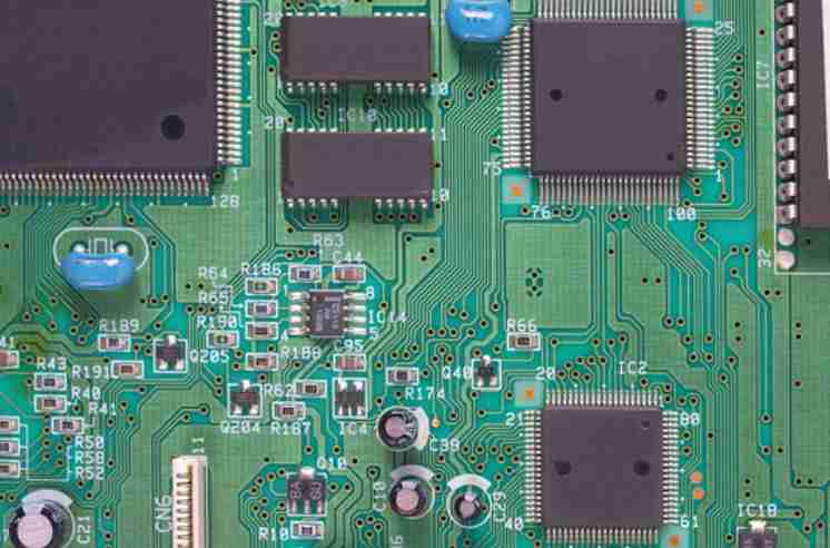
Higher density means that HDI designers must always keep in mind factors such as layout and spacing. Here are four tips to avoid common HDI PCB design mistakes:
1. Make space a priority
Considering space in the HDI-PCB design process is not just about compressing as many components as possible. First, the designer must ensure that the board will be properly maintained in the future. Determining the amount of space between specific parts and selecting additional space is a requirement. This can also make things simpler in the PCB manufacturing process. The through hole diameter, pad diameter and stitch width should be considered before implementation. Otherwise, the PCB may have to be completely redesigned, which requires more time, money and effort.
2. Understand the meaning of blind holes and buried holes
To make the most of the limited space, the HDI-PCB integrates blind and buried holes. Blind holes connect the outer and inner layers, but do not go through the entire board. Burials connect multiple inner layers, but do not pass through the outer layers. Blind hole and embedded through hole are different from traditional through hole in practicability and practicality, and have a great impact on the overall design of PCB. Designers must keep through-holes in mind because they affect not only the way the board is constructed, but also signal performance depending on its location and position.
3. Avoid solder-related problems
Solder can cause multiple HDI-PCB problems if the designer is not careful. For example, through holes in the pad may draw solder away from specific components, resulting in poor connections. One way to solve this problem is to avoid using through holes in the pad. Unfortunately, depending on the design of the HDI PCB and its purpose, sometimes this is not possible. In this case, covering the pad with through-holes and a welding mask eliminates the problem. However, using a welded mask can cause its own complications. Solder masks with large openings can allow large amounts of solder to reach the board, resulting in logical deletion or pin disconnection. It is crucial for the designer to monitor potential solder problems before the design begins.
4. Include in design review
This applies to all PCB design projects, but is of particular concern in HDI. It can be difficult for designers to examine their work and find small mistakes. This becomes doubly difficult when designers use higher density components. Combining advice and perspective from other designers, technicians, etc., is a strategic way to correct small mistakes before they become bigger and more costly problems. Skipping design reviews to meet tight deadlines may save some immediate time, but in the end, reviews are an ideal way to save time and money.
5, integrated circuit block power pin increase high frequency lotus root capacitance
Each integrated circuit block power pin to add a high frequency dropout capacitor. Increasing the high frequency decoupling capacitance of the power supply pin can effectively restrain the interference of high frequency harmonics on the power supply pin.
6. Avoid loops formed by cable routing
All kinds of high-frequency signals should not form a loop. If it cannot be avoided, the loop area should be as small as possible.
7, must ensure good signal impedance matching
In the process of signal transmission, when the impedance is not matched, the signal will be reflected in the transmission channel, and the reflection will make the synthesized signal form over in pulse, resulting in signal fluctuation near the logical threshold.

The fundamental way to eliminate the reflection is to make the impedance of the transmission signal good match, because the load impedance and the transmission line characteristic impedance difference is larger the reflection is larger, so it should be as far as possible to make the signal transmission line characteristic impedance and load impedance equal. At the same time, it should be noted that the transmission line on the PCB should not have mutations or corners, and the impedance of each point of the transmission line should be kept continuous as far as possible, otherwise there will be reflections between the sections of the transmission line. This requires that the following wiring rules must be observed when high-speed PCB wiring is carried out:
(1) LVDS wiring rules. Require LVDS signal differential wiring, line width 7mil, line distance 6mil, the purpose is to control HDMI differential signal pair impedance of 100+-15% ohm;
(2) USB wiring rules. USB signals are required to be routed differently, with a line width of 10mil, line distance of 6mil, and ground and signal line distance of 6mil.
(3) HDMI wiring rules. HDMI signal differential wiring, line width of 10mil, line distance of 6mil, each two groups of HDMI differential signal pairs spacing more than 20mil;
(4) DDR wiring rules. Signal cables must be of the same width and equidistant from each other. Cables must meet the 2W principle to reduce crosstalk between signals. For DDR2 high-speed devices or later, cables must be of the same length to ensure signal impedance matching.
Maintain the integrity of signal transmission and prevent the "ground projectile phenomenon" caused by the division of ground wire.
Design of high frequency PCB wiring
Feb 14,2023


Just upload Gerber files, BOM files and design files, and the KINGFORD team will provide a complete quotation within 24h.