
Professional PCB manufacturing and assembly
Building 6, Zone 3, Yuekang Road,Bao'an District, Shenzhen, China
+86-13410863085Mon.-Sat.08:00-20:00

Today, kingford will introduce two PCBA packaging technologies, namely plug-in packaging technology and surface adhesive packaging technology.
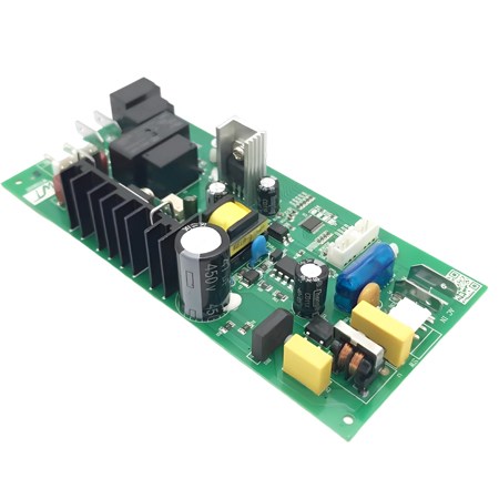
Circuit board
1. Plug-in packaging technology
The technique of placing the parts on one side of the board and welding the pins on the other side is called plug-in packaging. Such parts take up a lot of space and require a hole to be drilled for each pin. So their joints actually take up space on both sides, and the solder joints are larger. Interfaces like wire sockets and things like that have to be pressure resistant, so they're usually THT packages
2. Surface adhesive packaging technology
Parts that use surface adhesive packaging are welded to the same side as the part. This technique does not weld holes in the PCB for each pin. SMT also has smaller parts than THT, and PCB boards using SMT technology are much more densely packed than PCB boards using THT parts. SMT packaging parts are also cheaper than THT's. So most of today's PCB is SMT, naturally not surprising.
Because the solder joints and parts are very small, it is very difficult to use manual welding. However, if you consider the current PCBA assembly is fully automatic, this problem will only occur when repairing parts.

2. Precautions and operation skills of circuit board design
General new engineers for circuit board design skills are not very familiar, therefore, understand some circuit board design knowledge is quite necessary, let kingford for you to introduce the circuit board design matters needing attention and operation skills.
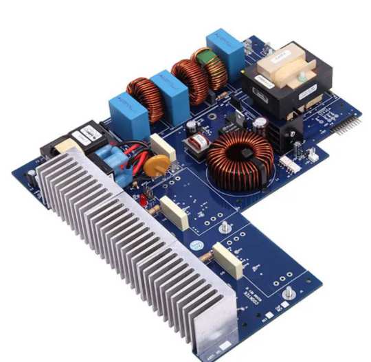
Circuit board
1. The definition of processing level should be clear
When there is no clear place in the document, be sure to find a professional engineer to check, so as to reduce the chance of plate making errors.
2, the distance between the copper foil and the outer frame can not be too close
Large area of copper foil from the outer frame distance to maintain at least 0.2 mm spacing.
3. Do not use filler blocks to draw welding pads
Drawing pad with filler block is OK in circuit board design, but it can not be used in processing, because such pad can not directly generate solder resistance.
4, the electric formation can not flower welding pad and line coexistence
The ground is different from the actual printed plate image, they are opposite, all the lines are barrier lines, can not leave a gap, otherwise it is easy to lead to short circuit of the power supply.
5. The pad should not be too short
If the pad is too short, it is easy to misposition the test pin. Because of the dense pad, the spacing between the feet is very small, and the pad is very thin. When installing the test needle, it must be staggered up and down to complete, otherwise this situation will occur.
6, the pad can not overlap
Pad overlap is easy to lead to scrap phenomenon in the drilling process, so the pad must not overlap.
The above is about the "circuit board design precautions and operation skills" introduction, I hope to have some help to you, more PCBA information please pay attention to the content of the site updates! Shenzhen kingford is a professional PCBA processing enterprise, with fully automatic SMT production line and wave soldering, for you to open the whole production and quality testing process, find us, you belong to have your own electronic processing plant!


Just upload Gerber files, BOM files and design files, and the KINGFORD team will provide a complete quotation within 24h.