
Professional PCB manufacturing and assembly
Building 6, Zone 3, Yuekang Road,Bao'an District, Shenzhen, China
+86-13410863085Mon.-Sat.08:00-20:00


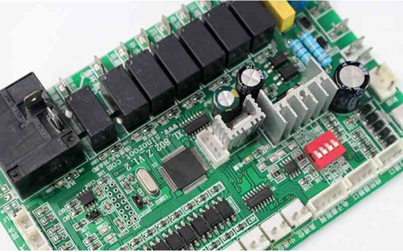
Complex PCB, often from the design of the solution.
A seemingly rational PCB design, thanks to a deep control area and copper plating on the board, produced a bizarre scene during welding, where the board bubbled in layers. Is the processing of the design, or ignoring the welding process, please see today's case analysis.
Small wind in a product company to do PCB design, she is a beautiful girl, her mouth light, she is confident and calm, she elegant and do not lose the sun.
Piao recently in the design of a PCB, in the area near the edge of the board, there is a device is 0.4 mm higher than the board, but the product has strict requirements on the thickness of PCB, the device can not exceed the thickness of PCB, otherwise the assembly will be due to the thickness of the device exceeds the standard, and can not be normally put into the cavity.
After discussion with structural engineers, small floating decided to solve the problem from PCB design of the device beyond the plate thickness.
Firstly, a sinking area is designed on PCB, and the device is sunk to meet the assembly requirements of the product through PCB forming depth control.
After the discussion with the process engineer of the factory, the scheme is feasible.
She quickly adjusted the layering scheme and everything was perfect.
Suddenly, she had a bright idea that she could electroplating copper in the sinking area of PCB, which also improved the heat dissipation of the product to some extent.
At the moment, she was in a good mood. Considering the influence of processing and copper plating thickness, she hummed a little song and made the following remarks on the original PCB drawing.
The PCB file was soon sent to the factory, and the board was also produced according to Piao's design.
Waiting is a long and painful process.
There is hope for waiting called waiting, there is no hope for waiting called suffering.
Fortunately, the wait was soon over.
The finished PCB board was soon handed over to Piao.
Tomorrow will be the day when PCB goes online for welding and assembly.
Tomorrow is also destined to be an extraordinary day.
Watch the board slowly from the automatic loading machine into the assembly journey.
Solder paste printing, SPI, high-speed patch, pre-furnace inspection, only the last step, reflow welding over 12 temperature zone.
A miracle is about to happen. It's time to see it.
Small floating at this moment of the mood, like just opened Coca Cola, taking the cheerful bubbles.
There are always surprises and surprises. Sometimes you wait so long for the stars to appear that you look up and the day comes...
The moment the board came out from the furnace, small floating could not believe his eyes, have you ever seen the north steamed bread?
Yes, at this time the board on the step area, like filled with a just out of the pot steamed bread.
It was bubbling golden and golden
All the disappointment comes from their own blind expectations, small floating can not understand where the problem is.
All of a sudden, she saw a familiar figure in the workshop, handsome, graceful, that is the world known as know-it-all, omnipotent PCB process engineer Wang Daxian.
Small gone with the wind originally dim eyes in the moment full of look, she ran to Wang Daxian cheerful, excited to say:
"Big Fairy, help me see what the problem is."
The fairy picked up the bubbling board, looked at it for a moment, smiled slightly, and then said:
"Xiao Piao, PCB board in the most powerful copper foil separation curse, copper foil and substrate adhesion is not enough, after the heat impact of layered bubbles."
"Can you explain it in detail?" Small floating quickly asked.
The fairy said, "Girl, this is a complicated matter. I will make it short. It starts with the pressing of the PCB."
PCB pressing has three musketeers - copper foil, core, PP.
Hard plate commonly used copper foil is electroplated with copper sulfate solution, it is smooth, we called the smooth surface, the other Side is rough crystal surface, called hairy (Matte Side), the two sides roughness is different, the rougher side can be treated with resin to produce a strong bonding force.
Prepreg is the abbreviation of Pre-pregnant. It is a kind of lamellar bonding material synthesized by resin and glass fiber cloth carrier.
It exists as a coiled solid at room temperature. When laminated, cut into sheets. During pressing, when the temperature inside the press reaches above its TG, after a period of time, it will slowly change from solid state to glass state, that is, (resin) into the shape of glue. Resin is a kind of thermosetting material which can undergo polymeric polymerization. It can be used as an adhesive between copper foil and fiberglass cloth.
Core is a combination of PP and copper foil after PP has been fully cured. It is completely cured after being pressed together by high temperature and high pressure vacuum. In the factory PCB processing, its shape and thickness is basically stable, there will be no big change. In the production of PCB, it has a variety of names, such as core board, core, substrate. In fact, it is a glass fiber cloth with epoxy resin and double-sided copper foil a mixture.
Below is a normal 6-ply lamination with copper foil top and bottom surfaces and PP and core in the middle. In the press through high temperature and high pressure vacuum,PP melting, the CORE and copper foil completely bonded together. When fully cured, it becomes what we call a multilayer circuit board.

The circuit board designed and produced by Piaopiata is in the PCB pressing and then on the board to do depth control treatment, and the depth control area, the circuit board has been completely cured, and then on the copper plating above it, the copper foil is simply deposited on the substrate, its binding force is not pressed when copper foil bonding force is good, at high temperature impact, plating copper and substrate layered foaming.
Master you said I was still a little dizzy, in the workshop Wang Daxian said for a long time, small floating still some do not understand.
At this time just off work, Wang Daxian pulled small wind to the factory park outside the bicycle repair stall, let small wind there to see Uncle Li tire. Uncle Li first picked up a file, grinding it hard on the tire, then coated it with glue, and finally pressed a piece of rubber on it. A moment later, the damaged tire was repaired. Then big fairy asked little Piao what you saw. Small wind excited said big fairy I understand, Uncle Li is really not easy, you see him sweating, I want to design a good artificial intelligence tire products, let uncle Li is not so tired. Big fairy moment to feel a breath does not come, hold for a long time, leisurely say a word, do not polish the tire, how to increase the tire and rubber binding force, after filling will leak.


Just upload Gerber files, BOM files and design files, and the KINGFORD team will provide a complete quotation within 24h.