
Professional PCB manufacturing and assembly
Building 6, Zone 3, Yuekang Road,Bao'an District, Shenzhen, China
+86-13410863085Mon.-Sat.08:00-20:00


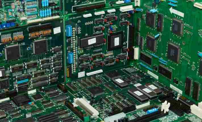
For the current printed circuit board (PCB) market, although the era of "any fool can make money" has gone forever, but due to the strong drive of intelligent terminals and automotive electronics, as well as the rapid rise of the Internet of things and wearable devices, PCB market still maintains a steady growth in the economic environment. For the current competition and survival of PCB enterprises, who can grasp the customer, product, technology, capacity, cost of these five factors, who can stand in the market. Therefore, whether considering from market demand or enterprise development, it is particularly important for PCB system design engineers to complete the design and timely delivery with low cost, fast and efficient.
However, as semiconductor technology is becoming more and more mature, packaging technology is also following the development of chip breakthroughs, single chip, single packaging equipment is no longer the mainstream, the traditional system electronic product design "Over the Wall: chip - package - circuit board" method will increase the overall cost of equipment, can not meet the current demand. So engineers have to deal with multiple chips and complex 3D packaging options, and do all this for multiple boards (platforms) at the same time. This requires system design engineers to integrate the knowledge of multiple disciplines, while taking into account the IC design, packaging and PCB system level design.
This is difficult for PCB system design engineers, says David Liens, business development manager of Mentor Graphics' system design division. Although IC design, packaging and PCB system design have standard specifications to follow and launched a design tool, however, such a design tool because only for IC design, so PCB system design engineers in the design, still must be for IC, packaging and PCB system pin path planning. The field of IC design and packaging is like an impenetrable wall for PCB system design engineers. It will take a long time to complete the design of the pin path at each stage, which will lengthen the time to market.

In view of this, Ming Guide International has introduced the latest Edition Package Integrator process. According to David Liens, it is the industry's broadest solution for IC design and manufacturing, packaging, and printed circuit board (PCB) co-design and optimization. The solution uses a unique virtual chip model concept that ensures IC, packaging, and PCB are optimized for each other to reduce packaging substrate and PCB costs by efficiently reducing layers, optimizing interconnect paths, and streamlining/automating control of the design process.
David Liens highlighted that the Edition Package Integrator product also provides the industry's first formal process for ball grid array (BGA) ball mapping planning and optimization. This process is defined according to user rules and is based on the concept of "smart pins". In addition, a groundbreaking multi-mode connection management system, combining hardware description Language (HDL), spreadsheets, and eschatology, provides cross-domain pin mapping and system-level cross-domain logic validation.
"Mentor Graphics fully recognizes the increasing complexity of electrical system design and manufacturing, especially for chip, package, and circuit board co-design," John Park, Division Solution Architect, Mentor Graphics SDD(System Design Division). "Our latest Edition Package Integrator process enables system designers to achieve optimal productivity by improving the overall quality and performance of advanced systems while saving time and cost."
In addition to the challenges facing system design engineers in large enterprises, PCB design engineers in small and medium-sized enterprises also encounter other "annoyances". Whether PCB, IC or other electronic design automation (EDA) software tools are usually quite expensive, built in the most complete, advanced functions, and these are generally large enterprise engineers can enjoy the "benefits"; Independent engineers who typically work in small and medium-sized enterprises or are part of individual teams within large enterprises (such as building prototypes, verifying reference designs, and performing manufacturing studies) are often limited to lower-priced, mid-range products. They are responsible for performing full process design, analysis and manufacturing data delivery tasks for PCB electronics. Engineers who worked on complex designs in the past had no choice but to embrace enterprise solutions, and many of them were unable to implement those solutions due to budget constraints and massive infrastructure requirements.
As the need to design electronics efficiently increases, this task often falls to the independent engineer responsible for carrying out the entire design process. The design process often involves more than schematic input and circuit board layout, and may require analysis of such factors as signal integrity, thermal simulation, mass-production feasibility design, and distribution network integrity. Also, depending on the enterprise, the complexity of the final product can range from simple to very complex.
To meet this demand, Ming Guide International has also launched three new PADS series. According to David Liens, the new PADS family meets the increasing design needs of electronics engineers and builds on previous experience with strong PADS technology, in some cases utilizing technologies from the market-leading Edition suite. Now, independent engineers can buy these products at great value, and use the unique capabilities of Mentor Graphics to improve design efficiency, improve product quality, reduce costs, and shorten the design cycle.
According to David Liens, these new products are classified as Standard, Standard enhanced, and professional: (1) PADS Standard- schematics and board designs with a central library, package creation wizard, and archive management capabilities. (2) PADS Standard Plus- In addition to the PADS Standard functions, there are advanced circuit constraint managers, high-speed circuit design and topology changes, creation and management of a central library of PCBS, signal/thermal/analog simulation support for Hyper Lynx, etc. (3) PADS Professional- In addition to the PADS Standard Plus capabilities, these include technologies used in Edition, such as AI sketch routing, 2D/3D real-time synchronous design, layout by functional module, device and Web browser, production preparation, and design review/comparison.
With a 41% market share in the PCB design software market, both the Edition Package Integrator process for the "system concept" and the new PADS family for independent engineers seeking efficient design capabilities, All of these are good news for the development of the design industry and PCB design engineers.


Just upload Gerber files, BOM files and design files, and the KINGFORD team will provide a complete quotation within 24h.