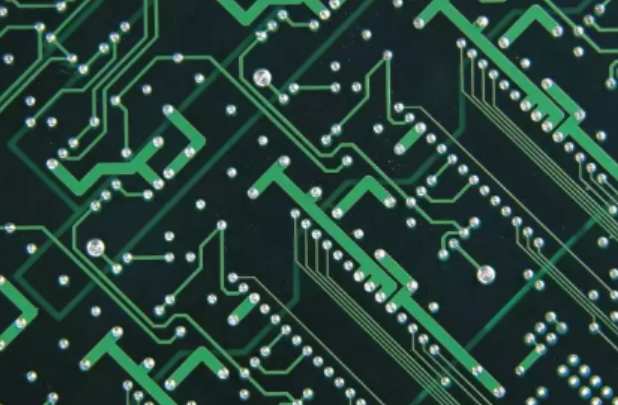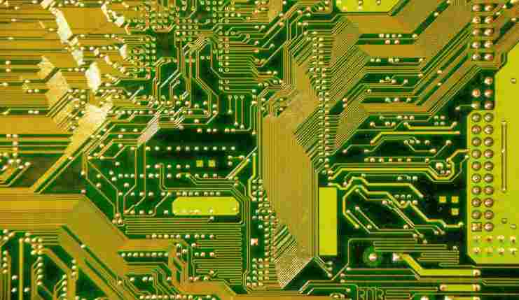
Manufacturing dry film for PCB is a difficult task that must be carried out in strict clean room conditions using a dedicated coating line. Such facilities are usually dominated by a few large companies, such as DuPont, Morton Nikko and Hitachi.
After coating and parts drying, the master roll is cut to the size required by the PCB manufacturer. To increase utilization, PCB companies must order the exact width required for panel sizes. If a different panel size is required, the reels need to be replaced, resulting in downtime and lost production. In warmer climates, the film must be stored in a controlled storage facility, which is an added cost.
The equipment used to laminate dry film (cutting paper laminates) is becoming increasingly complex and expensive to purchase and maintain. For example, CLS units can cost up to $200,000, while rubber laminates can cost up to $600 to place after deformation. Every 6-8 weeks.

Another problem with dry film is that PCB manufacturers must specify the exact film width to match the size of the copper sheet used, and changing film rolls to boards of different widths can result in expensive down time.
However, one of the disadvantages of thin dry film may be its adhesion to copper panels.
The copper sheet may appear flat to the naked eye, but upon closer inspection, a rough surface with dendritic (tree) appearance will be revealed. Everything looks fine until the printing plate enters the etching bath. Etching chemicals will enter below the dry film (micro-cracks) and effectively eat up the fine copper, creating an open circuit, which is usually only discovered after etching and cannot be examined because there are no visible signs.
Over the past decade, Rainbow has been working on chemistry and systems design to overcome the problems of the wet film method. Rainbow's proprietary liquid Resist and coating system, introduced at Productronica last year, addresses these issues by giving PCB manufacturers complete control over the treatment and control over liquid resist that flows easily, adheres tightly to the substrate surface and can be used at ambient temperatures.
Resist does not need to be dried prior to imaging.
The panel can still be treated because the resist coating has been protected by a layer of mylar film. The resist is first coated onto the polyester reel and then directly laminated onto the copper sheet, thereby leaving the protective polyester carrier on the resist transfer coating.
After laminating, the panel is "monolithic" to separate it from the carrier fibre network. The panel can then be exposed by any method, including DI/LDI.
Mixed paint
To complement the new generation of resist, the company has now introduced the Hybrid Coating Unit (CL21 Hybrid Coating Laminate Machine).CL21 makes it easy to handle wet resist and gives PCB manufacturers complete control over the printing process. A roll of polyester fiber is then laminated directly onto the copper sheet, leaving the polyester protective jacket on the resist transfer coating.
After laminating, the panel is "monolithic" to separate it from the carrier fibre network. The split panel can then be exposed by any method, including DI/LDI.
Coating thickness can range from 2 to 30 microns, and thinner resist are ideal for fine line printing. Part number and thickness can be changed in 2-3 minutes. The coating unit can be configured to coat a single - or double-sided panel, fibre-mesh, as an etching or coating resist.
When proprietary liquid resist is used in conjunction with CL coater, the intent is to save PCB manufacturers significant time and money, as well as improve the quality of the final product and reduce defects.
pcb design process
Know how to design a printed circuit board, a PCB is a key element of any electronic circuit design process. The layout and design of the PCB has a big impact on the way the circuit works, so if the PCB design is effective, then the circuit will perform more reliably within its specifications.
First, pcb design environment
For commercial development solutions, there may be CAD, computer aided design packages, required due to complexity. Even for students and amateurs, there are many very good packages, both free and available at a modest cost. Freeware provides basic functionality, while high-end software packages enable more facilities to be incorporated into the design: analog circuits, complex circuits, multilayer circuits, etc. As the speed of digital boards increases and RF designs reach higher and higher frequencies, the ability to perform simulations is becoming an increasing requirement.
Two, circuit schematic diagram
The first stage of PCB design and development is the schematic design of the circuit, which can be achieved in a variety of ways. Some pcb design software comes with schematic drawing. We import the schematic file into the pcb design tool to generate a "Netlist", grid table to connect each pin and connected device and circuit node together.
Three, pcb component initialization
Before proceeding to a detailed PCB design and layout, it is necessary to have a general idea of where the components will be located and whether there will be enough space on the board to contain all the required circuits. This will allow people to decide the number of layers needed for the board and whether there is enough space to contain all the circuits that might need to be carried out. Once a rough estimate of the space and approximate location of the components has been made, a more detailed component layout can be provided for PCB design. This can take into account aspects such as the proximity of devices that may need to communicate with each other, and other information relevant to any RF considerations. In order for a component to be incorporated into a PCB design, they must know all the relevant information about the component: the shape of the board, the aperture information, the distance area, and so on. Typically, several devices may share the same pin, so you do not need to enter this information for each component part number. Build a package library for all devices in the PCB design. This allows previously used components to be easily invoked.
Iv. Wiring
Once the basic components have been placed, the next stage of PCB design is to route the connections between all the components. The PCB software then routes according to the information in the Netlist table in the schematic. To achieve this, it will use the number of layers available for connections, created through holes as needed. Typically, one layer will be assigned as the GND layer and the other as the power plane. This not only reduces the noise level but also enables low source resistance connections for power. Wiring is time-consuming, especially for large designs that may have more than three or four thousand components. When wiring becomes difficult due to multi-component density, this can cause wiring to take a lot of time.
V. pcb file (gerber)
Output PCB layout picture information in the form of Gerber file. This format is the standard for PCB files, which are the form of CNC files used by photo plotters. In addition to the Gerber file, borehole information is generated as well as screen printing and photo saving information. A major factor in the cost of printed circuit boards is drilling. In any design, some holes are needed to hold it in place, as well as holes required for regular parts. However, to keep costs down, it is wise to use as few hole sizes as possible. This way, the drill bit will require less variation and time can be reduced.
PCB files are used in many areas of the manufacturing process. It is not only used in the manufacture of the PCB itself, but the documents will also be used in other areas of the manufacturing process. Such as the production of steel mesh, SMT, ICT testing, needle testing home, etc. Above is the whole process of PCB design products, PCB design is not just drawing design.


