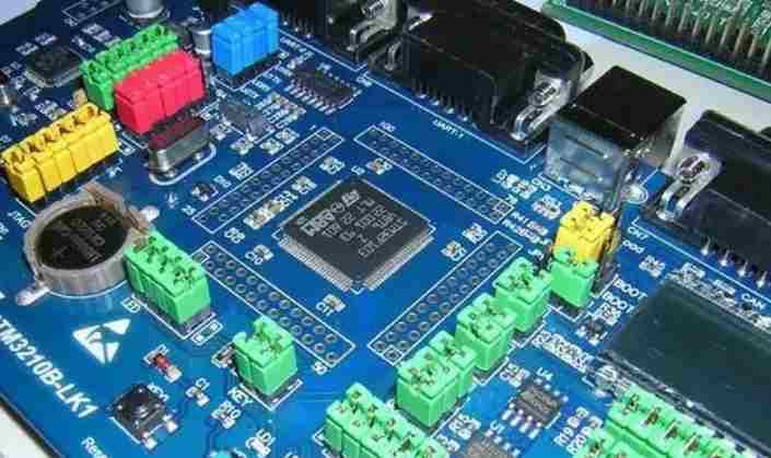
Virtually every electronic product consists of one or more printed circuit boards (PCBS). PCBS immobilize IC and other components and interconnect them. A large number of PCBS were created for portable electronic devices, computers and entertainment devices. They are also used for testing equipment, manufacturing and spacecraft. Eventually, almost every EE will have to design a pcb, which is not something taught in school. However, engineers, technicians and even novice pcb designers can create high-quality PCB designs for any purpose and be confident that the results will meet or exceed the goals. Again, these designs can be completed on schedule and within budget while meeting the design requirements. Designers need to consider the necessary documentation, pcb design steps and strategies, and final inspection.

Basic design process
The ideal pcb design begins with requirements analysis and continues until the final delivery (Figure 1). After the project is obtained, a pcb requirements analysis should be determined, which covers the functionality of the pcb design, the functionality that the pcb must have and perform, interconnections with other circuits, layout, and approximate final dimensions. The ambient temperature range and issues related to the working environment should be addressed and used in the material of choice specified for the pcb. The selection of components and pcb materials should be mindful of all predictable and potential forms of threat to ensure that the pcb will work properly during its service life. The circuit schematic diagram is drawn according to the schematic diagram. This detailed diagram shows the electrical implementation of each function of the pcb. After schematics are drawn, the final pcb layout should be completed and areas designated for each schematic block of the circuit.
Bill of materials
A bill of Materials (BOM) must be generated when you create the schematic diagram. Components in a circuit should be selected by analyzing the limiting operating voltage and current levels at each node of the circuit while tolerance criteria are considered. After selecting an electrically satisfactory component, each component should be reconsidered based on availability, budget and size. The BOM must always be synchronized with the schematic diagram. The BOM requires the quantity of each component, reference code, value (ohm, farad, etc.), manufacturer part number and pcb footprint. These five requirements are critical because they define how much is required for each part, explain the identification and circuit location while accurately describing each circuit element to be purchased and replaced, and explain the dimensions of each part to be used for area estimation. It should be a concise list describing each circuit element, and too much information might make library development and management too complicated.
pcb file
The pcb documentation shall include hardware dimensional drawings, schematics, BOM, layout files, component placement files, assembly drawings and instructions, and Gerber file sets. A Gerber file set is a pcb term for the layout output file that pcb manufacturers use to create a pcb. The complete Gerber file includes output files generated from the circuit board layout file: Silkscreen up and down, solder stop top and bottom, all metal layers, solder paste top and bottom, component diagram (XY coordinates), top and bottom of assembly drawing, drill file, turn hole diagram, FAB outline (Dimensions, special features), netsheet file. Special features included in FAB profiles include, but are not limited to, notches, bevels, backfill pads (for BGA-type IC packages with multiple pins under them), blind/buried through-holes, surface finish and smoothness, hole tolerances, number of layers, etc.
Schematic details
The schematic controls the project, so accuracy and completeness are critical to success. They contain the information necessary for the circuit to function correctly. The schematic should include sufficient design details, such as pin numbers, names, component values and ratings.
Each schematic symbol has a manufacturer's part number used to determine price and specifications. Package specification Determines the package size of each component. The first step should be to ensure that the bare copper of each pin is placed in the correct position and is slightly larger (3 to 20mil) than the component pins, depending on the available area and welding method. When designing a pcb package, consider assembly and follow the manufacturer's recommended pcb package. Some components are microencapsulated, so there is no excess copper margin. Even in these cases, a stop electrode of 2.5 to 3mil should be applied between each pin on the board. Follow the rule of 10. The small through hole has a final diameter of 10mil, plus a 10mil pad ring. The line should be 10mil or longer from the edge of the plate. The cable spacing is 10 Mil (5mil air gap, 5mil cable width, 1 oz copper). For holes 40 mil in diameter or larger, pad rings should be added to improve reliability. For the outer copper plane from the plane to the pin, an additional clearance of 15 to 25mil beyond the design rules should be provided. This reduces the risk of bridging all solder joints.
The next step is to place the components and locate them based on thermal management, function, and electrical noise factors. After the outline of the component and the location of the interconnect are assigned, the first component placement step begins. After each component is placed, it should be reviewed and adjusted immediately to facilitate wiring and optimize performance. Layout and packaging sizes are often reconsidered and changes are made at this point based on size and cost. Components that absorb more than 10 mW or conduct more than 10 mA should be considered powerful enough to take into account other thermal and electrical factors. Sensitive signals should be separated from noise sources through a flat surface and kept impedance controlled. The power management module uses the ground plane or the power plane for heat flow. Make high current connections according to acceptable connection voltage drops. Layer conversions with high current paths should use two to four throughholes at each layer conversion and multiple throughholes at layer conversions to improve reliability, reduce resistance and inductance losses, and improve thermal conductivity.


