
Professional PCB manufacturing and assembly
Building 6, Zone 3, Yuekang Road,Bao'an District, Shenzhen, China
+86-13410863085Mon.-Sat.08:00-20:00

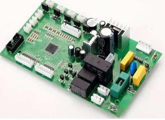
What we need to take into account is the size of the circuit board. If the size is relatively large, the printed line is long, whICh will bring about the increase of resistance and the decrease of anti-interference ability. If it is too SMAll, it will lead to poor heat dissipation of the circuit board, and the adjacent line is susceptible to interference. Finally, we can rationally arrange the circuit board according to the function of the circuit. Generally, we should abide by the following rules. Next, kingford will explain how to design anti-interference circuit boards and how to print solder paste on circuit boards.1. How to print solder paste on circuit board
Print the solder paste on the circuit board and then connect the electron IC parts to the circuit board through reflow. It is the most common method in the electronic manufacturing industry. The printing of solder paste is actually a bit like painting on the wall. However, in order to more accurately apply the solder paste to a certain position and control the amount of solder paste, a more refined special steel plate (stencil) must be used to control the printing of solder paste.
solder paste printing is the basis of solder on the PCB board, and the position and amount of solder paste is more key. You often see that solder paste printing is not good, which will cause solder short circuit and solder empty. But really want to print solder paste well, also have to consider the following factors:
1. Type of Squeegee: Suitable squeegee should be selected for solder paste printing according to the characteristics of different solder paste or red glue. Currently, squeegee used in solder paste printing is made of stainless steel.
2, scraper Angle: scraper scraping solder paste Angle, generally between 45 ~ 60 degrees.
3. Scraper pressure: Scraper pressure will affect the volume of solder paste. In principle, other conditions remain the same, the greater the pressure of the scraper, the less solder paste will be. Because the pressure is large, is equal to the gap between the steel plate and the circuit board compressed.
4. Scraper speed: The speed of scraper will also directly affect the shape and quantity of solder paste printing, and also directly affect the quality of solder printing. Generally, the speed of the scraper will be set between 20 and 80mm/s. In principle, the speed of the scraper must match the viscosity of the solder paste. The better the fluidity of the solder paste, the faster the speed of the scraper should be, otherwise it will be easy to seepage. In general, the faster the speed of the scraper, the less the solder paste will be.
5, the demoulding speed of the steel plate: if the demoulding speed is too fast, it is easy to cause the phenomenon of solder paste wire drawing or point drawing, which may affect the effect of parts.
6. Whether to use vacuum block? The vacuum seat can help the circuit board to stick smoothly in the fixed position, strengthen the close fit of the steel plate and the circuit board. Sometimes a multi-purpose thimble/ejector can be used instead of a vacuum block for products that are only produced once and in small quantities.
7. Is the circuit board deformed (warapge)? Deformed circuit boards will let solder paste printed uneven, in most cases will cause short circuit.
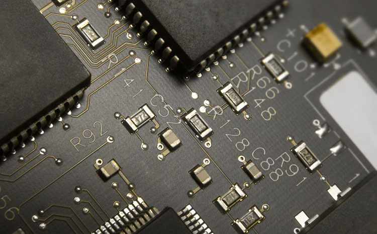
8. stencil aperture. The opening of steel plate directly affects the quality of solder paste printing, which needs to be explained in a special chapter.

2. How to design anti-interference circuit board
Circuit board in the process of operation, often because of various interference circuit board can not work normally, most of these interference is caused by the circuit design is not reasonable, so in the design of circuit board, we need to pay attention to the reasonable layout design of the circuit. In the layout of the circuit board, the first thing we need to take into account is the size of the circuit board, if the size is relatively large, the printed line is long, which will bring about the increase of resistance, anti-interference ability decline, if too small, it will lead to the heat dissipation of the circuit board is not good, and the adjacent line is susceptible to interference, under the circumstances of determining the size of the circuit board, We need to first determine the location of special components, and finally we can rationally layout the circuit board according to the function of the circuit. Generally, the following rules should be observed.
1. We should shorten the wire distance between high-frequency components as far as possible, through this method to reduce their distribution parameters and electromagnetic interference between each other, for those easy to interfere with the components can not be too close, input and output components should be far away.
2. As there may be a high potential difference between some components or wires on the circuit board, we should appropriately increase the distance between them to avoid accidental short circuit due to discharge. Components with high voltage should be arranged as far as possible in places that are not easily touched by the hand during debugging.
3 For the weight of more than 15g components, should be fixed with a support, and then welding. Those large and heavy, heat components, should not be instalLED on the printed board, but should be installed on the chassis bottom, and should consider the problem of heat dissipation. The heat sensitive element should be far away from the heating element.
4. For potentiometer, adjustable inductance coil, variable capacitor, micro switch and other adjustable components layout should consider the structural requirements of the whole machine. If the machine adjustment, should be placed above the printed board for easy to adjust the place; If the outside of the machine adjustment, its position to adjust the knob on the chassis panel position.
5. For devices with weak anti-noise ability and large power supply changes when the device is turned off, such as RAM and ROM memory devices, the advanced and backward coupling capacitor should be directly connected between the power cord and the ground wire of the chip.
6. Power line design according to the size of the printed circuit board current, try to increase the width of the power line, reduce the loop resistance. At the same time, the direction of the power cord and ground wire is consistent with the direction of data transmission, which helps to enhance the anti-noise capability.
7. The ground cable should be as thick as possible. If the grounding wire is very thin, the grounding potential will change with the change of current, so that the noise resistance performance is reduced. The ground wire should therefore be thickened so that it can pass through three times the allowable current on the printed board. If possible, the ground cable should be at least 2 mm to 3mm. Circuit board how to carry out anti-interference needs to consider the problem from many aspects, the above introduction is just a SIMple introduction to some common anti-interference operation, in the actual operation needs to be a combination of personal experience and function to achieve anti-interference operation.
PCB design Layout Guide for engineers
Feb 07,2023


Just upload Gerber files, BOM files and design files, and the KINGFORD team will provide a complete quotation within 24h.