
Professional PCB manufacturing and assembly
Building 6, Zone 3, Yuekang Road,Bao'an District, Shenzhen, China
+86-13410863085Mon.-Sat.08:00-20:00

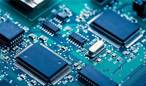
As the "mother of electronic products" PCB board is the key and basic link in the whole industrial chain of electronic products. As PCB production materials, is the foundation of the foundation, can be said to be the modern electronics industry of the building of sand. With the rapid development of downstream applications such as Internet of Things technology, 5G communication and automotive electronics, the PCB industry is developing rapidly.
According to China Business Information Network, the market capacity of PCB industry in China is expected to reach 38.15 billion US dollars in 2022, with an annual compound growth rate of about 5%, but the medium and low end printed circuit board are mainly, which indicates that the high frequency and high speed PCB board and its material market has further development space in China.
What is a high frequency high speed PCB board?
Generally speaking, high frequency high speed PCB board refers to the frequency of 1GHz above the printed circuit board, this definition may not be the same in the industry. Its physical performance, precision, technical parameters requirements are very high, often used in communication system, automotive ADAS system, satellite communication system, radio system and other fields.

In addition, a device has a digital processing and interface component in addition to the RF system. Driven by consumer demand for faster Internet connections, mobile high-definition video and the Internet of Things, PCBS must also support high-speed digital data transmission. IoT, 5G and commercial applications such as big data centers, as well as increasingly personal applications, continue to push the boundaries of digital communication system speed. According to statistics, the bandwidth of high-speed digital systems is almost doubling every three years driven by data rates.
What are the important parameters of high frequency and high speed PCB?
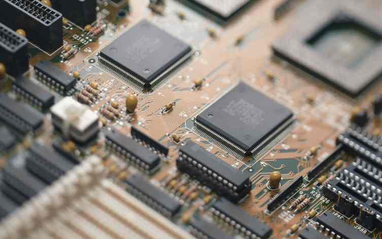
The production process of high frequency and high speed PCB board is basically the same as that of ordinary PCB board. The key point to achieve high frequency and high speed is the properties of raw materials, that is, the characteristic parameters of raw materials. The main material of high frequency and high speed PCB board is high frequency and high speed copper-covered board, its core requirements are to have low dielectric constant (Dk) and low dielectric loss factor (Df). In addition to ensuring low Dk and Df, the consistency of Dk parameters is also one of the important factors to measure the quality of PCB board. In addition, there is an important parameter is the impedance characteristics of PCB board and some other physical characteristics.
High frequency high speed circuit board substrate dielectric constant (Dk) must be small and stable, generally speaking, the smaller the better, the signal transmission rate and the square root of the material dielectric constant is inversely proportional, high dielectric constant easy to cause signal transmission delay.
High frequency and high speed circuit board substrate material dielectric loss (Df) must be small, which mainly affects the quality of signal transmission, the smaller the dielectric loss, the smaller the signal loss.
Impedance of high frequency high-speed circuit board -- actually refers to the resistance and the parameters of reactance, impedance control is the most basic principle for us to do high-speed design, because PCB circuit to consider plug installation of electronic components, plug into consideration after the electrical performance and signal transmission performance, so it is inevitable that the lower the impedance, the better. In general, every major board factory will ensure a certain degree of impedance error during PCB processing.
High frequency high speed circuit board substrate water absorption should be low, high water absorption will cause dielectric constant and dielectric loss when damp.
How to measure the parameters of high frequency and high speed PCB and materials?
As we mentioned just now, the production process of high-frequency and high-speed PCB is basically the same as that of ordinary PCB, and its characteristic parameters mainly depend on the characteristic parameters of PCB materials. Therefore, in order to produce PCB board in line with the requirements, in addition to using the corresponding process, the more important is to use the appropriate synthetic materials of PCB. Therefore, as PCB manufacturers, R & D designers should first test PCB materials and confirm characteristic parameters; Before the production of the template, the PCB board was modeled through the design simulation software, and the characteristic parameters were fitted, so as to generate the PCB template. Then the template was verified and tested, and the continuous iteration was carried out. After meeting the requirements, the mass production was carried out. In the process of mass production, PCB board is tested by random inspection or full inspection as required.

Testing part of PCB production process
As a PCB material provider, it is necessary to understand the characteristics of its own materials, and make specifications of the characteristics and parameters of the materials provided to customers, so as to confirm whether they can meet the requirements of customers' PCB characteristics. Therefore, they need to test the raw materials, which include a variety of wave fiber cloth materials and a variety of resin materials or synthetic copper coated plate.
Dk/Df test of PCB materials
In order to meet the signal integrity requirements of different applications, in addition to the analysis of the dielectric constant Dk and dielectric loss Df of the material itself to achieve effective PCB board design, the PCB also needs to be tested for S parameter and TDR impedance, which involves many technical details, such as instrument calibration, Fixture extraction and embedding (AFR) and transmission line simulation test.
These testing schemes have greatly promoted the development and production of PCB materials by upstream and downstream manufacturers in our PCB industry, increased their market share, improved their technical level, and accelerated the import substitution of products.


Just upload Gerber files, BOM files and design files, and the KINGFORD team will provide a complete quotation within 24h.