
Professional PCB manufacturing and assembly
Building 6, Zone 3, Yuekang Road,Bao'an District, Shenzhen, China
+86-13410863085Mon.-Sat.08:00-20:00

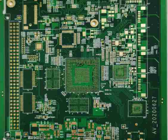
A Printed circuit board (PCB) is printed in almost every type of electronic device. If there are electronic parts in a device, they are all mounted on PCBS of different sizes. In addition to fixing various small parts, the main function of PCB is to provide electrical connection between the above parts. As electronic equipment becomes more and more complex, the need for more and more parts, PCB above the circuit and parts are more and more dense. A standard PCB looks something like this. Bare Board (with no parts attached) is also often referred to as a "Printed Wiring Board (PWB)".
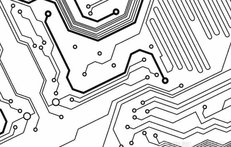
The substrate of the board itself is made of an insulating, non-bendable material. The small wire material that can be seen on the surface is copper foil. Originally, copper foil is covered on the whole board, but in the manufacturing process, the middle part is etched away, and the remaining part becomes a network of small lines. These circuits are called conductor patterns, or wiring, and are used to provide circuit connections for parts on the PCB.
To secure the parts to the PCB, we solder their pins directly to the wiring. On the most basic PCB (single panel), the parts are concentrated on one side and the wires on the other. In this way, we need to make holes in the board so that the connector can go through the board to the other side, so the connector of the part is welded to the other side. Because of this, the front and back of the PCB are respectively called Component Side and Solder Side.

If there are parts on the PCB that can be removed or put back on after the PCB is made, the Socket is used when the part is installed. As the socket is directly welded on the board, the parts can be arbitrarily disassembled. I see ZIF (Zero Insertion Force) sockets that allow parts (cpus) to be inserted and removed easily. A retaining rod next to the socket to hold the part in place after you plug it in.
To connect two PCBS to each other, we usually use the edge connector known as the "golden finger". The finger contains a number of exposed copper pads that are actually part of the PCB wiring. Usually to connect, we insert the gold finger on one PCB into the appropriate Slot on the other PCB (generally called an expansion Slot). In computers, interface cards such as video cards, sound cards, and the like are connected to the main board by the gold finger.
The green or brown on the PCB is the color of solder mask. This layer is an insulating protective layer that protects the copper wire and prevents parts from being welded in incorrect places. A silk screen will be printed on top of the solder resistance layer. It is usually printed with words and symbols (mostly white) to indicate the position of the parts on the board. Screen printing is also known as legend.
High frequency PCB layout and wiring 10 tips
Feb 06,2023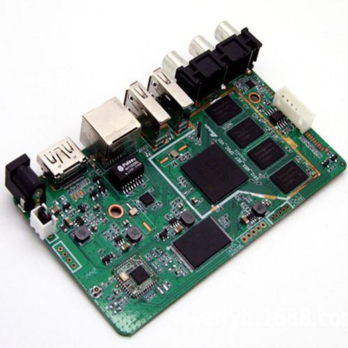


Just upload Gerber files, BOM files and design files, and the KINGFORD team will provide a complete quotation within 24h.