
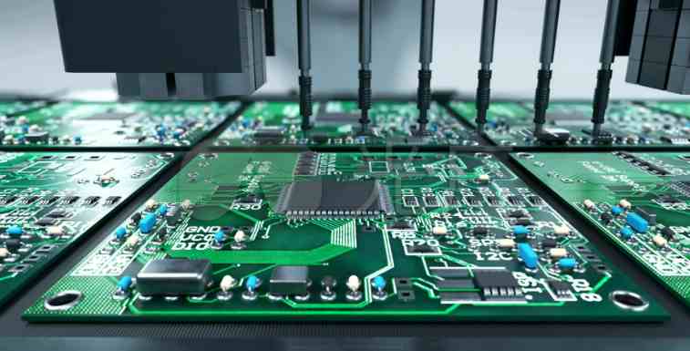
Professional PCB manufacturing and assembly
Building 6, Zone 3, Yuekang Road,Bao'an District, Shenzhen, China
+86-13410863085Mon.-Sat.08:00-20:00

For some customers, the design is seriously non-standard, and they can't tell which is pad and which is via. Sometimes the conductive hole is treated with pad, and sometimes the key hole is treated with via. The design is confused, which leads to more mistakes. As for the current situation of the circuit board, some of the engineers dealing with Philin, because of the non-standard design documents of the customer, and go wrong, help the customer to modify the documents, the non-standard design is correct, with their own experience to deal with the engineering data, which leads to and contributes to the non-standard design of the customer, Jialicuang once again stated that the last time you did the right, does not mean your file is right! All engineers must pay attention to the design standards and specifications! Jialichuang will again strictly require all the engineers to deal with Philin, as far as possible to maintain the status of customer documents! As far as possible to do according to the design specification and standard processing, not according to the so-called experience processing! To reflect the problem, so as to improve the level of design engineers for some Jialichuang will make unremitting efforts to change this situation!
This article focuses on conductive holes, keyholes, and the connection between protel /pads/ and geber files
Conducting hole: via

Key hole: pad
A few problems are particularly likely to arise:
1) pad mixed with via, resulting in problems
1) When your files are pads or protel, send them to the factory and ask for the cover oil. Please note that you need to carefully check if your pad is also useful via, otherwise you will get green oil on your PAD hole, which will lead to the failure of welding. The plug-in hole must be sprayed with tin. Why did you cover the oil and how did I use it? Please check the file when saying this, whether it was designed by pad or via!
2) When your files are pads or protel, send the files to the factory, and the order requirement is through hole cover oil. Many customers use pad (plug-in holes) to represent conductive holes, which leads to the opening of your conductive holes. Maybe you want through hole cover oil, and then there may be a dispute that what I want is conductive hole cover oil. Then please check your document design!
2) via in the conversion process, due to the design is not standard or you are not clear about the conversion gerber setting rules, resulting in problems
3) When you send the gerber file, the factory can't tell which are the holes and which are the key holes. The only thing that can be identified is processing according to the file, which will help the welding layer and then there is a window! The gerber you sent out is the film file, and the factory has no way to check whether it is conductive hole or keyhole. Please check the gerber file to see if it is helpful for welding layer. If it is, open the window, if it is not, cover the oil
Three: How to design hole cover oil in protel or pads! ------ This is the most standard practice, if the design standard, you must not go wrong!
In protel, there is a tenting option in the via property, if you check it, it must be cap oil then you turn out all of the cap oil. In pads, the way to turn files in pads is to go through the hole (via) cap method:
When exporting soldermask, i.e., solder layer, just check the vias below soldermask top ---- to indicate that you pass through the window. If you do not check, pass through the hole cover oil
To sum up: pad according to pad, this is the plug-in hole, via you have two choices, if you provide the original file, you can choose when placing the order, if you provide the gerber file, please check whether the gerber file meets your requirements!
The improvement of various production processes ensures the quality and delivery time of PCB proofing products
With the "copper plating" process put into use, our company's various production lines have been established, through the introduction of production technical personnel, increase the training and education of production line staff, to ensure the production quality of each process, ensure the on-time delivery of each product. Judging from the feedback of our customers, our current PCB samples are beautiful in appearance, bright in color, stable in quality and on time in delivery, which have been unanimously praised by our customers!


Just upload Gerber files, BOM files and design files, and the KINGFORD team will provide a complete quotation within 24h.