
Professional PCB manufacturing and assembly
Building 6, Zone 3, Yuekang Road,Bao'an District, Shenzhen, China
+86-13410863085Mon.-Sat.08:00-20:00

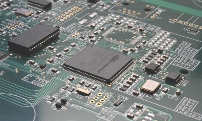
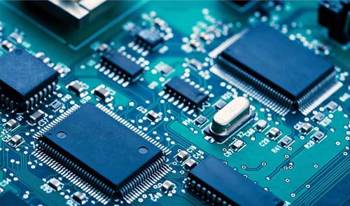
In PCB design, generally we are very concerned about signal quality, but sometimes we tend to limit the study on the signal line, and treat the power and ground as the ideal situation, although this can simplify the problem, but in high-speed design, this simplification is not feasible. Although the more immediate result of circuit design is the signal integrity, we must not neglect the power supply integrity design. Because the power supply integrity directly affects the final PCB board signal integrity. Power supply integrity and signal integrity are closely related, and in many cases, the main cause of signal distortion is the power system. For example, the ground rebound noise is too big, the design of decoupling capacitor is not appropriate, the loop influence is very serious, the segmentation of the ground plane of multiple power sources is not good, the formation design is not reasonable, the current is not uniform and so on.
1. Power distribution system
The integrity design of the power supply is very complicated, but how to control the impedance between the power supply and the ground plane is the key to the design. Theoretically, the lower the impedance between power systems, the better. The lower the impedance, the smaller the noise amplitude, the smaller the voltage loss. In the actual design, we can determine the target impedance we want to achieve by specifying the maximum voltage and power supply range, and then make the impedance of each part of the power system (related to frequency) approximate the target impedance by adjusting the relevant factors in the circuit.
2. Ground rebound
When the edge rate of a high-speed device is less than 0.5ns, the data exchange rate from a high-volume data bus is particularly fast, creating a power instability problem when it creates strong ripples in the power layer that affect the signal. When the current through the ground loop changes, the inductance of the loop will generate a voltage. When the rising edge is shortened, the current change rate increases and the ground rebound voltage increases. At this point, the ground plane (ground) is no longer an ideal zero level, and the power supply is not an ideal DC potential. As the number of simultaneous switching gates increases, the ground bounce becomes more severe. For a 128-bit bus, there may be 50_100 I/O lines switching along the same clock edge. At this point, the inductance of both the power supply and the ground loop feedback to the simultaneously switching I/O driver must be as low as possible, otherwise, the static connected to the same ground will appear as a voltage brush. Ground bounces can occur anywhere, such as on chips, packages, connectors, or circuit boards, which can lead to power integrity issues.
From the point of view of technology development, the rising edge of the device will only decrease and the width of the bus will only increase. The only way to keep ground bouncing in acceptable is to reduce the power supply and ground distribution inductance. For chips, this means moving to an array of wafers, placing as much power and ground as possible, and making the wires to the package as short as possible to reduce inductance. For packaging, it means moving layer packaging, so that the ground planes of the power supply are closer together, as used in BGA packaging. For connectors, this means using more ground pins or redesigning the connector to have internal power and ground planes, such as ribbon cords based on connectors. For PCB circuit boards, this means bringing adjacent power sources and ground planes as close together as possible. Since inductance is proportional to length, making the connection between power and ground as short as possible will reduce ground noise.
3. Decoupling capacitor
We all know that adding some capacitance between the power supply and the ground can reduce the noise of the system, but how much capacitance do you put on the printed circuit board? How much capacity is appropriate for each capacitor? Where is each capacitor better placed? We don't really think about these kinds of issues, we just follow the designer's experience, and sometimes even think that less capacitance is better. In the high-speed design, we must consider the capacitance of the parasitic parameters, quantitative calculation of the number of decoupling capacitors and the capacity of each capacitor and the specific position of the placement, to ensure that the impedance of the system within the control range, a basic principle is the need of decoupling capacitors, one can not be less, redundant capacitors, one do not.
Pcb inhibits reflection interference
Feb 02,2023


Just upload Gerber files, BOM files and design files, and the KINGFORD team will provide a complete quotation within 24h.