
Professional PCB manufacturing and assembly
Building 6, Zone 3, Yuekang Road,Bao'an District, Shenzhen, China
+86-13410863085Mon.-Sat.08:00-20:00

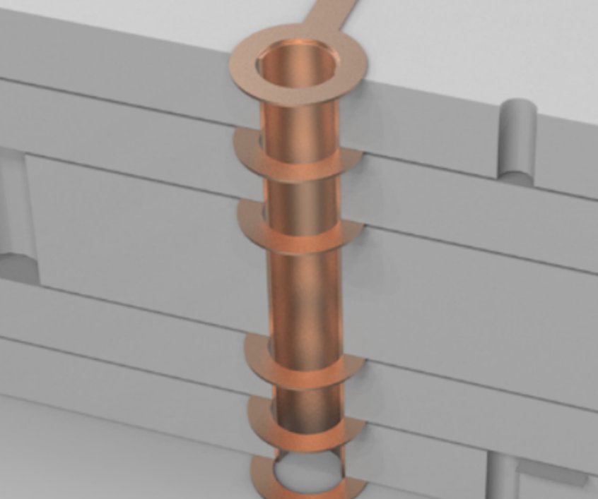
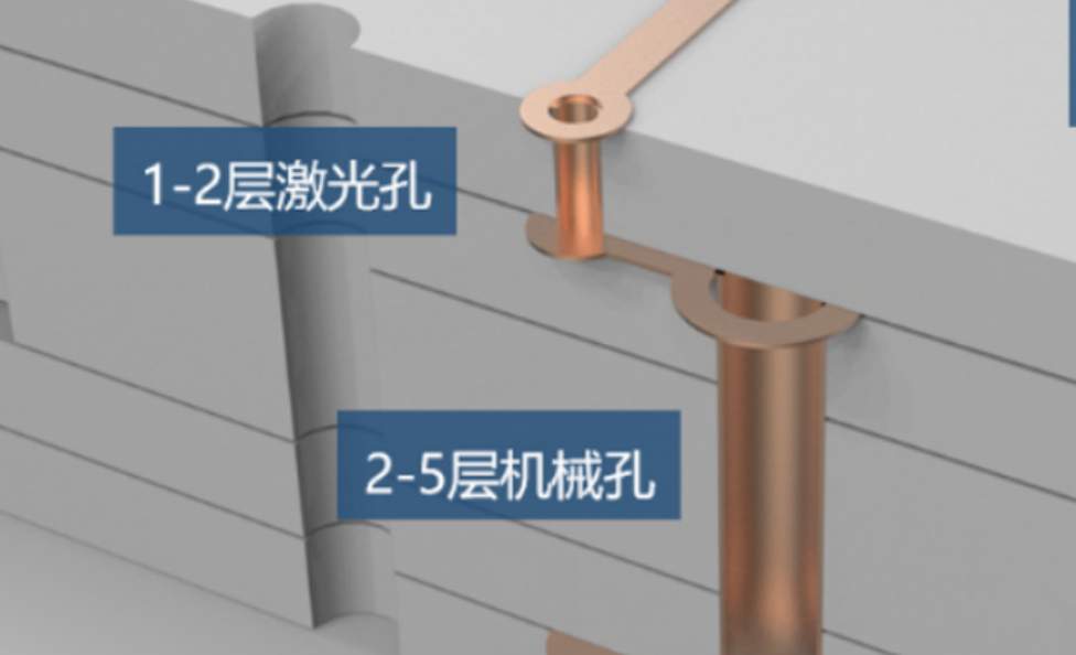
The PCB hole is mainly composed of the hole, the bright plate area around the hole, and a part of the power layer isolation area. In high speed PCB design, it is often necessary to use multi-layer PCB, and the hole is multi-original.
An important factor in PCB design, high-speed PCB multilayer board, signals from one layer of interconnect to another layer of interconnect need to be connected through holes. So, high speed
What problems should be paid attention to in PCB hole design?
1, from the point of view of favorable dry heat dissipation, PCB circuit board is best installed upright, the distance between the boards should not be less than 2cm.
2, for the use of free convection air cooling equipment, it is best to arrange integrated circuits in a longitudinal way; For devices that use forced air cooling, it is best to put the integrated circuit in horizontal rectangle
Type arrangement:
3, the same piece of PCB circuit board on the device as far as possible according to its heat size and heat dissipation degree partition arrangement: small heat or poor heat resistance of the device (such as small signal transistor, etc.) in cold
But the flow of the most upstream: large heat or good heat resistance devices (such as power transistors, etc.) in the cooling flow of the most downstream.
4. In the horizontal direction, the high-power devices are arranged as close as possible to the edge of the PCB circuit board, so as to shorten the heat transfer path; In the vertical direction, the high power device as close as possible to the PCB board
The upper part is arranged in order to reduce the influence of the work of the device on the temperature of other devices.
5, more sensitive to temperature devices had better be placed in the lowest temperature area (such as the bottom of the device), multiple devices had better be staggered in the horizontal layout.
6, in the design to study the air flow path, reasonable configuration of devices or printed circuit boards: to avoid leaving a large airspace in a certain area.
7. A lot of practice shows that the temperature of printed circuit can be effectively reduced by adopting a reasonable arrangement of devices.

1, choose a reasonable hole size. For more than a dozen general density PCB design, with drilling bright disk, POWER isolation area selection of more than 1,000 feet of mold, people 0.25mm, 0.51mm, 0.91mm: for some high density PCB, can also use 0.20mm, 0.46mm, 0.86mm through the hole, Non-through-through holes can also be attempted. For through-holes of power supplies or ground wires, larger sizes can be considered to reduce impedance.
2. The bigger the power quarantine zone, thWhat problems should be paid attention to in high speed PCB hole design?
The PCB hole is mainly composed of the hole, the bright plate area around the hole, and a part of the POWER layer isolation area. In high speed PCB design, it is often necessary to use multi-layer PCB, and the hole is multi-original.
An important factor in PCB design, high-speed PCB multilayer board, signals from one layer of interconnect to another layer of interconnect need to be connected through holes. So, high speed
pcb proofing
Feb 01,2023


Just upload Gerber files, BOM files and design files, and the KINGFORD team will provide a complete quotation within 24h.