
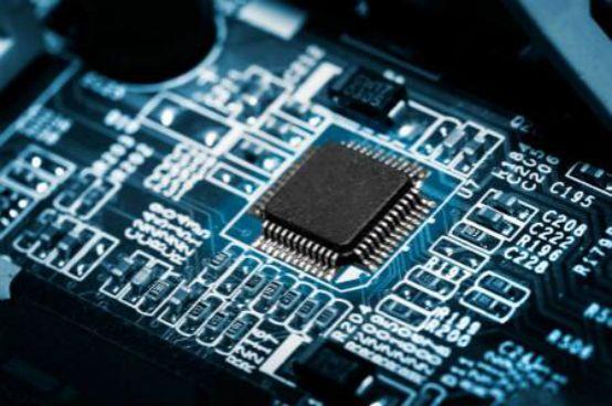
Professional PCB manufacturing and assembly
Building 6, Zone 3, Yuekang Road,Bao'an District, Shenzhen, China
+86-13410863085Mon.-Sat.08:00-20:00

After the PCB size is determined, the pendulum position of the special component is determined.
According to the function unit, the layout of all components of the circuit board.

The location of special components shall comply with the following principles in the layout:
1. Shorten the connection between high-frequency components as far as possible, and try to reduce their distribution parameters and electromagnetic interference between each other. Components susceptible to interference should not be too close to each other, and input and output should be as far away as possible.
2 Some components or wires may have a higher potential difference, should increase their distance, so as to avoid accidental short circuit caused by discharge. High voltage components should be placed out of reach of hands as far as possible.
3, the weight of more than 15G components, can be fixed by support, and then welding. Those heavy and hot components, should not be placed on the circuit board, should be placed on the bottom of the main case, and consider the heat dissipation problem. Heat-sensitive components should be kept away from heat-generating components.
4, and the potentiometer, adjustable inductance coil, variable capacitor, micro switch and other adjustable components layout should consider the structure of the whole board requirements, some often used switch, in the case of the structure allows, should be placed in the hand easy access to the place. Component layout to balance, density, can not be top-heavy. The success of a product, one is to pay attention to the internal quality. The second is to take into account the overall beauty, both are more perfect board, in order to become a successful product.
A transmission line is defined as a signal line with signal backflow (composed of two wires of a certain length, one is the signal propagation path and the other is the signal return path). A common transmission line is the line on our PCB board.
How long is the transmission line on the PCB board?
This is related to the propagation speed of the signal, which is 6in/ns in the copper wire bar on the FR4 plate. Simply put, as long as the round-trip time of the signal on the circuit is greater than the rise time of the signal, the circuit on the PCB should be treated as a transmission line. Let's see what happens when the signal travels over a long stretch of track. Assume that a 60-inch PCB is routed. The return path is the ground plane of the inner layer of the PCB near the signal cable. The signal cable and the ground plane are open at the far end. Resistive damage in PCB design of power supply is a very common open-circuit fault. It is rare for the resistance value to become large, and rarely for the resistance value to become small.

1. TOP/BOTTOM PASTE (top/bottom paste) :
This layer is generally used for solder paste in SMT reflow soldering process of patch components. It has nothing to do with the printed board manufacturer's board. It can be deleted when GERBER is exported and can be retained as default in PCB design.
2. TOP/BOTTOM OVERLAY (top/bottom Silk-screen layer) :
Design for a variety of silk screen logo, such as component digit, character, trademark, etc.
3. MECHANICAL LAYERS:Design for PCB mechanical shape, default LAYER1 is the shape layer. Other LAYER2/3/4 etc. can be used for mechanical dimensioning or special purposes. For example, when some boards need to make conductive carbon oil, LAYER2/3/4 etc. can be used, but the purpose of the layer must be clearly marked on the same floor.
A little experience on line width and copper laying through holes
We generally have a common sense when drawing PCB, that is, use thick lines (such as 50mil, or even above) where the current is high, and use thin lines (such as 10mil) for signals with low current.
For some electromechanical control systems, sometimes the instantaneous current flowing through the wire can reach more than 100A, so the relatively thin wire will certainly cause problems.
A basic rule of thumb is 10A/ mm2, that is, 10A for a cable with a cross-sectional area of 1 mm2. If the wire width is too thin, it will burn out when a large current passes through it.
Of course, the current burning wire should also follow the energy formula: Q = I*I*t. For example, for a 10A current wire, a 100A current burr suddenly appears, with a duration of us level, then the 30mil wire is sure to be able to withstand.
(Which brings up another problem? The stray inductance of the wire, the burr will produce a strong reverse electromotive force under the action of this inductance, which may damage other devices. The thinner and longer the wire, the larger the stray inductance, so in practice, the length of the wire should be considered.) Copper substrate includes metal layer, bonding layer (insulation layer), conductive wire layer, and all three factors are indispensable.
Other matters to be dealt with before casting the board
I. QA review within the group
After receiving the process, QA in the group should first confirm that the designer has conducted sufficient self-check. If the process is not completed, QA will return to the process and ask the designer to submit the process again after completion.
Review and record review results, handling suggestions, etc. The process is returned to the designer if the review fails.
QA review comments within the group should also be entered into the board Design Review record database.
Two, short circuit fault inspection
1. Single point grounding; Plane layer hollowing out; Care should be taken when modifying the treatment of welding pad hot pad, and the treatment results should be written in the source division of the design file, which is conducive to self-inspection and QA review and the next plate modification.
2. When the electric stratum of P software is divided negatively, it must be checked carefully. The method of checking the electric formation negative with P software is as follows: set the Nenets assigned to the same layer to different colors.
Only all elements of the layer to be checked are displayed.
Check whether the network crosses the partition zone (different colors are in the same partition zone). If no, the partition succeeds.
If there is cross-division, you need to edit the NETHERMAL properties of cross-zone pad and through-hole so that they do not generate flowerplates in this area, and then ensure the connectivity through wiring.
3, there are Windows or slots must be added to the forbidden area of the line, to prevent the line to dig off, resulting in a break. Structural element.
4. DRC must be set correctly and all DRC checks must be turned on.
In the nickel plating solution at higher temperature, the obtained nickel coating has low internal stress and good ductility. The general operating temperature is maintained at 55~60 degrees.
Due to the thin thickness of the copper layer in PCB, the oxidized copper will become a bad conductor of electricity, which will greatly damage the electrical performance of the entire PCB. PCB proofing of circuit board
Friends who have done PCB know that PCB in SMT processing, there are usually 3 methods: manual, semi-automatic, automatic. All manual is to brush steel mesh, placing electronic components are manual operation. Semi-automatic refers to the manual brush steel mesh, placing electronic components on the automatic placement machine. Automatic refers to the brush steel mesh and placing electronic components are fully automatic machine equipment.
Design method of PCB design Mark point:
1. Enter the package editor and place a round patch pad with a diameter of 1mm on the top layer;
2. A copper foil hollowed out area with a diameter of 3mm is placed on the top layer;
3. Place a copper foil with a diameter of 3mm on the top solder resistance layer;
4. Save it.

The disposal method of waste circuit board
Jan 29,2023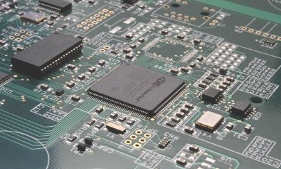


Just upload Gerber files, BOM files and design files, and the KINGFORD team will provide a complete quotation within 24h.