
Professional PCB manufacturing and assembly
Building 6, Zone 3, Yuekang Road,Bao'an District, Shenzhen, China
+86-13410863085Mon.-Sat.08:00-20:00

From the type of power switch selected to the layout of the printed circuit board, many design decisions affect the robustness of high power inverter design.
One Evaluate the type of power switch.
One of the first decisions to make is the type of power switch to use. Power switches have unique features and requirements such as voltage limits, temperature ranges, and operating frequencies that will drive many design decisions for high-power inverters, including which type of grid driver to use.

The four main types of power switches are:
1.Silicon MOSFET
2. Insulated gate bipolar transistor (IGBT)
3. Silicon Carbide (SiC)
4. gallium nitride (GaN)
two Consider operating voltage requirements
Operating voltage is another factor to consider. Designers must assess the maximum voltage exposed to the system under normal conditions and ensure that the grid drivers and power switches can meet these power requirements. For grid drivers, the operating voltage rating will exceed the maximum expected peak voltage. For switches, the rule of thumb is that the maximum expected voltage should be less than 80% of the rated voltage of the equipment family.
Grid drivers and power switches have critical protection requirements that must be addressed in the design. For example, undervoltage problems generate heat and efficiency losses. Overvoltage will cause switch damage. Fortunately, these problems can be mitigated with solutions such as desaturation detection, the use of the Miller effect to prevent switch parasitization, and careful PCB layout techniques.
Application with PCB layout
Three. Consider the dependencies of your application.
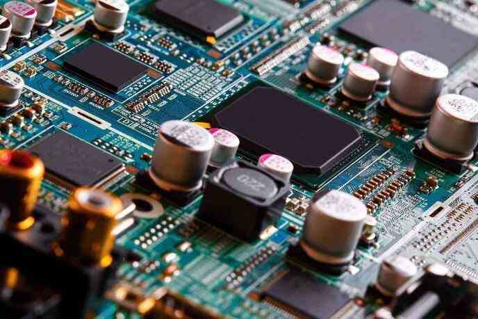
A stable, high-power application, such as a steady-running industrial motor inverter, may not require much protection. Conversely, dynamic applications, such as electric vehicle traction inverters, may require extensive system protection. PCB board layout is also an important factor to consider when designing power electronic circuits, as it determines the performance, efficiency and reliability of power circuits. Well-planned PCB layouts reduce parasitic inductors and capacitors, improving reliability and efficiency.
Four. Consider how to power the secondary side of the half-bridge device.
This task can be done discreetly or in combination. When you design your high power inverter, look for power switching technology and grid drivers that suit the operating voltage required for your system application. Consider the critical protection requirements and select a gate driver that provides the appropriate solution.
Do power amplifier board mainly pay attention to the following points:
1, meet enough current carrying (choose copper thickness and laminated);
2. Meet safety requirements (electrical clearance and creepage distance);
With that said, let's first talk about two concepts: electrical gap and creepage distance.
The shortest distance measured along the air between two adjacent conductors or between one conductor and the surface of an adjacent motor housing;
Creepage distance: The shortest distance between two adjacent conductors or one conductor and adjacent motor housing surfaces along the non-insulating surface measured.
Safety reference:
In the process of PCB design, if the creepage distance cannot be satisfied, we should increase the creepage distance between conductors by grooving.
We have two kinds of grooving; One is to directly use a washing knife for grooving, its minimum width is 0.8mm. The other method is to use the method of drilling, this is can drill out the minimum slot width can be 0.2mm;
When it comes to the primary wiring of transformers, their ground should be designed in a single-point grounding manner.
The primary end of the transformer control MOS tube to be hollowed out, banned (heat is too large), because the optocoupler is a low voltage to control the high voltage of a device, so all the optocoupler need to use grooves to control its creepage spacing.

The safe distance between two different places should also be considered; For example, PE and GND,
If the potential difference between two components or networks is large, electrical insulation needs to be considered. The clearance safety voltage in the general environment is 200V/mm, which is 5.08V/mil. Therefore, when there are both high-voltage and low-voltage circuits on the same circuit board, it is necessary to pay special attention to adequate safety spacing. When there is a high voltage circuit and a low voltage circuit, special attention needs to be paid to adequate safety spacing. Here we have to consider, the above we talk about is just a theoretical value, but in fact, we in the design process, 220V high pressure he generally have a gap spacing of about 2mm; The 500V high voltage is designed for 4~5mm; The distance here refers to the distance between all conductors and conductors to the wire hole pad device.
One of the most important indicators in the amp boardis the current, if the serial current can not be controlled, then the PCB is scrapped products.
Skills required for RF circuit board engineers
Jan 28,2023


Just upload Gerber files, BOM files and design files, and the KINGFORD team will provide a complete quotation within 24h.