
Professional PCB manufacturing and assembly
Building 6, Zone 3, Yuekang Road,Bao'an District, Shenzhen, China
+86-13410863085Mon.-Sat.08:00-20:00

The circuit board manufacturer explains the key points of the circuit board ALIVH process
Circuit board manufacturer, circuit board design, PCBA processing manufacturer explain the key points of circuit board ALIVH process for you
1: The selection of insulating dielectric materials must meet the requirements of the functional characteristics of the substrate, with high TG and low dielectric constant. Aramide nonwovens currently used are reinforced semi curing sheet materials, which are characterized by light weight. Low dielectric constant, small thermal expansion coefficient and good smoothness. In particular, it has a negative coefficient of thermal expansion (CTE), which is matched with the CTE of the chip by adjusting the proportion of its composition with the epoxy resin to control the coefficient of thermal expansion of the substrate.
2: Select conductive adhesive matching the characteristics of epoxy resin. The plug hole conductive adhesive used shall have small shrinkage, that is, less volatile matter or its CTE shall match the CTE of the core plate (at least less than 35ppm). It has high conductivity and thermal conductivity, and has high heat resistance or resistance to welding thermal shock.
3: The size and shape of the stencil mesh shall be reasonably made according to the size and shape of the through hole diameter of the core plate to ensure that the blocked conductive adhesive can form a convex semicircle shape.
4: The size, shape and configuration of metal particles in the conductive adhesive shall be reasonably selected, and the resin system shall be optimized to ensure the formation of a conductive adhesive material with low viscosity for plugging high-density through holes and actually "zero" shrinkage.
5: Improve the flatness of the surface: a good grinding process must be selected, and the outstanding conductive adhesive must be ground to form a good, stain free surface to be machined that is consistent with the surface.
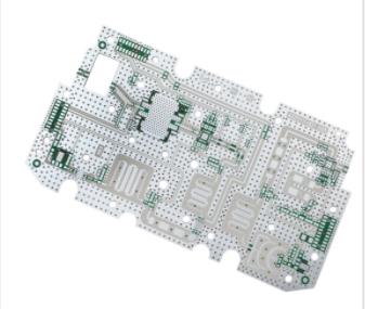
The basic level printed circuit board manufactured by this technology is characterized by fewer layers, high assembly density, simple design and convenient manufacturing, and has been widely used in portable communication systems.
With the development and change of microelectronics technology, new packaging forms such as BGA, CSP and MCM have emerged in addition to the thin chip and fine spacing of semiconductor devices at present. There are great changes around the technology of manufacturing multilayer boards.
In particular, it is necessary to adapt to the improvement of signal speed. The material selection of the laminated multilayer board and its insulating medium have already had the original glass cloth epoxy resin, and the newly developed insulating materials such as FR-4 with lower dielectric constant, thermosetting resin PDO resin, and polyimide resin based BT resin have been used instead. Due to environmental requirements, bromine flame retardants or halogen-free insulating materials have been developed to reduce the direct impact on the environment.
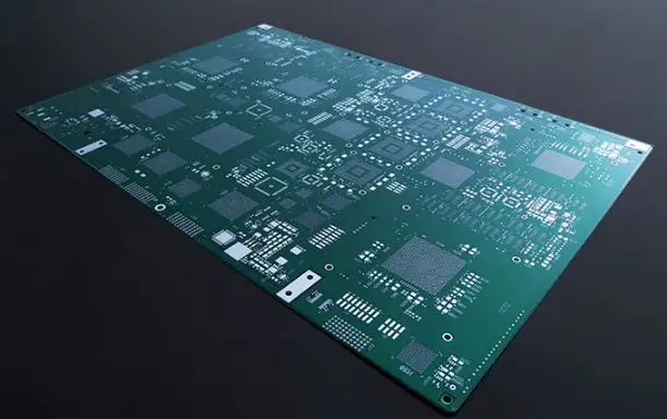
It is known from the current production process that the multilayer board wiring graphic design technology has reached the miniaturization level of 50/50UM conductor line width/spacing, and can pass 5 printed wires between the lead out pins of the integrated circuit. In order to adapt to the adoption of BGA, CSP and other new types of packaging, a new solder precoating process has been developed, which can form solder spots with arbitrary height and consistent size on narrow spacing for assembly.
The new technology of laminated multilayer board, which has developed several processes, among which ALIVH structure is one. The utility model mainly solves the problem that the interlayer connection of the conventional multilayer board is processed by mechanical drilling, chemical processing and optical processing for through hole processing and electroplating. The components used for assembly also need through holes, which is a waste of the effective area of the printed circuit board and directly affects the miniaturization of electronic products. With this process, the circuit density is high, the wire width and spacing can be reduced by more than 50/50um, and the through-hole diameter can also be less than 0.15mm. Of course, this requirement will make full use of the area under the device mark on the surface of the multilayer board for interlayer connection in the process and design. In this way, the effective area of the PCB can be reduced. Due to the short wiring distance, it is particularly suitable for high-speed circuits. PCB manufacturers, PCB designers and PCBA manufacturers will explain the key points of the circuit board ALIVH process to you.


Just upload Gerber files, BOM files and design files, and the KINGFORD team will provide a complete quotation within 24h.