
Professional PCB manufacturing and assembly
Building 6, Zone 3, Yuekang Road,Bao'an District, Shenzhen, China
+86-13410863085Mon.-Sat.08:00-20:00

Detailed explanation of five major trends of PCB technology development
PCB manufacturing, PCB design and PCBA processing manufacturers will explain the five major trends of PCB technology development in detail
Electronic equipment requires high performance, high speed, light weight and miniaturization. As a multidisciplinary industry, pcb circuit board is the most critical technology of high-end electronic equipment. In PCB products, no matter rigid, flexible, rigid flex multilayer boards, as well as module substrates used for IC packaging substrates, have made great contributions to high-end electronic equipment. PCB industry plays an important role in electronic interconnection technology.
In the 21st century, mankind has entered a highly information society, and PCB is an indispensable pillar in the information industry.
Recalling the hard journey of China's PCB over the past 50 years, today it has written a glorious page in the history of PCB development in the world.
With regard to the current development trend of PCB technology, I have the following views:
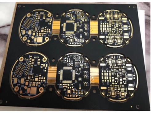
1、 Developing along the road of high-density interconnection technology (HDI)
As HDI embodies the most advanced technology of contemporary PCB, it brings fine wiring and micro aperture to PCB. Mobile phone (mobile phone), one of the electronic products of HDI multilayer board application terminal, is a model of HDI's cutting-edge development technology. In the mobile phone, the PCB main board fine wire (50 μ m~75 μ m/50 μ m~75 μ m. Conductor width/spacing) has become the mainstream, in addition, the thickness of conductive layer and plate is thin; The miniaturization of conductive patterns brings high-density and high-performance electronic equipment.
For more than 20 years, HDI has promoted the development of mobile phones, led the development of LSI and CSP chips (packaging) for information processing and basic frequency control functions, and also promoted the development of PCB. Therefore, it is necessary to develop along the HDI road.
2、 Component embedding technology has strong vitality
The formation of semiconductor devices (called active components), electronic components (called passive components) or passive component functions "component embedded PCB" in the inner layer of PCB has begun to be mass produced. Component embedded technology is a huge change in PCB functional integrated circuits, but to develop it must solve the simulation design method, and the production technology and inspection of quality and reliability assurance are urgent.
We need to increase resource investment in systems including design, equipment, detection and simulation to maintain strong vitality.
3、 Material development in PCB should be further improved
Whether rigid PCB or flexible PCB materials, with the global lead-free electronic products, it is required that these materials must have higher heat resistance. Therefore, new types of high Tg, small thermal expansion coefficient, small dielectric constant, and excellent dielectric loss tangent materials continue to emerge.
4、 Photoelectric PCB has broad prospects
It uses optical path layer and circuit layer to transmit signals. The key of this new technology is to make optical path layer (optical waveguide layer). It is an organic polymer formed by lithography, laser ablation, reactive ion etching and other methods. At present, the technology has been industrialized in Japan and the United States.
5、 Manufacturing process shall be updated and advanced equipment shall be introduced
1. Manufacturing process
HDI manufacturing has become mature and tends to be perfect. With the development of PCB technology, although the manufacturing methods commonly used in the past are still dominant, low-cost processes such as additive and semi additive have begun to emerge.
Using nanotechnology to metallize holes and form PCB conductive patterns at the same time, a new flexible board manufacturing process is developed.
High reliability, high quality printing method, ink-jet PCB technology.
2. Advanced equipment
Production of fine wires, new high-resolution photomask and exposure devices, and laser direct exposure devices.
Uniform coating equipment.
Manufacturing and installation equipment and facilities for embedded production components (passive active components). PCB manufacturing, PCB design and PCBA processing manufacturers will explain the five major trends of PCB technology development in detail.
Summarize the causes of PCB welding defects
Nov 25,2022


Just upload Gerber files, BOM files and design files, and the KINGFORD team will provide a complete quotation within 24h.