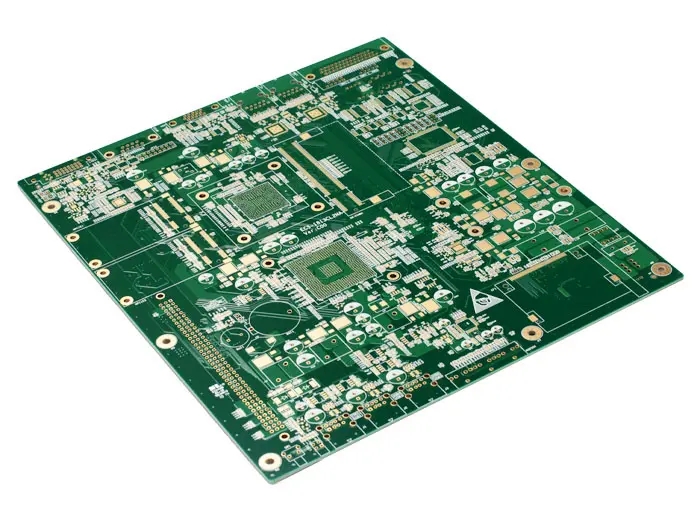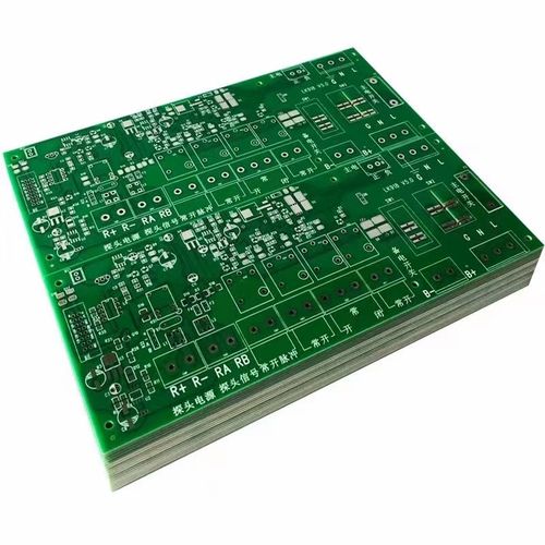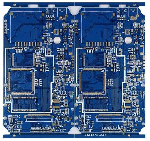
Must master the surface plating (coating) process of printed circuit board
Circuit board manufacturing, circuit board design and PCBA processing manufacturers explain the plating (coating) process on the surface of printed circuit boards that must be mastered
1、 Plating (coating) method for printed circuit board surface: a. Electroplating method. b. Electroless plating.
2、 Common elements of PCB surface coating:
A. Nickel, element symbol Ni, atomic weight 58.7, density 8.88g/cm3, electrochemical equivalent of Ni2+1.095g/AH.
b. Gold, element symbol Au, atomic weight 197, density 19.32g/cm3, electrochemical equivalent of Au+0.1226g/A • m.
c. Tin, element symbol Sn, atomic weight 118.69.
d. Silver, element symbol Ag, atomic weight 107.88.
e. Palladium, element symbol Pd, atomic weight 106.4.
3、 Plating overview:
a. Nickel: The nickel coating used for printed circuit board is divided into semi bright nickel (also known as low stress nickel or dumb nickel) and bright nickel. It is mainly used as the bottom layer of plate or plug gold plating, and can also be used as the surface layer as required. The coating thickness shall not be less than 2~2.5 according to IPC-6012 (1996) standard μ m。 The nickel coating shall be uniform and fine, with low porosity and good ductility, and the low stress nickel coating shall be suitable for brazing or pressure welding.
b. Gold: The gold plating layer used for PCB production is divided into two categories; Gold plating on board and gold plating on plug.
1) Gold plating on the board: The gold plating layer on the board is 24K pure gold with columnar structure, which has excellent conductivity and weldability. Plating thickness 0.01~0.05 μ m。
The gold plating layer on the board is made of low stress nickel or bright nickel as the bottom layer. The thickness of the nickel plating layer is 3-51xm. The nickel plating layer acts as a barrier layer between gold and copper, which can prevent the mutual diffusion between gold and copper and prevent copper from penetrating the gold surface. The existence of nickel layer is equivalent to improving the hardness of gold coating.

The gold plating layer on the board is not only the protective layer of alkaline etching, but also the final surface coating of IC aluminum wire bonding and button type printed circuit board.
2) Gold plating of plug: Gold plating of plug is also called hard gold plating, commonly known as "golden finger". It is an alloy coating containing alloy elements such as Co, Ni, Fe, Sb, etc. Its hardness and wear resistance are higher than those of pure gold coating. The hard gold coating has a layered structure. The gold plating layer of plug used for printed circuit board is generally 0.5~1.5 μ M or thicker. Alloy element content ≤ 0.2%. Gold plated plug is used for highly stable and reliable electrical contact connection; The coating thickness, wear resistance and porosity are required.
The hard gold coating uses low stress nickel as the barrier layer to prevent the mutual diffusion between gold and copper. In order to improve the adhesion of the hard gold coating and reduce the porosity, as well as to protect the plating solution and reduce pollution, a pure gold layer of 0.02~0.05p, m should be plated between the nickel layer and the hard gold layer.
c. Tin: Electroless tin plating on PCB bare copper plate is also a solderable coating that has received widespread attention in recent years.
Electroless tin plating on copper substrate is essentially chemical tin dipping, which is a replacement reaction between copper and complex tin ions in the plating solution to generate tin coating. When the copper surface is completely covered by tin, the reaction stops.
d. Silver: Electroless silver coating can be both soldered and "bonded" (pressure welding), so it is widely valued. The essence of the electroless silver coating is also silver immersion. The standard electrode potential of copper is 0Cu+/Cu=0.51 V, and the standard electrode potential of silver is 0Ag+/Ag=0.799 V. Therefore, copper can replace silver ions in the solution and form a silver layer on the copper surface: Ag++Cu → Cu++Ag To control the reaction rate, the Ag+in the solution will exist in the form of complex ions. When the copper surface is completely covered or the copper in the solution reaches a certain concentration, the reaction is ended.
e. Palladium: Electroless Pd plating is an ideal copper and nickel protective layer on PCB, which can be welded and "bonded". It can be directly plated on copper, and because Pd has autocatalytic ability, the coating can be long and thick. Its thickness can reach 0.08~0.2 μ m. It can also be plated on the electroless nickel coating. Pd layer has high heat resistance, stability and can withstand multiple thermal shocks.
During assembly welding, for Ni/Au coating, when the gold coating contacts with the molten solder, the gold is melted into the solder to form AuSn4. When the weight ratio of the solder reaches 3%, the solder will become brittle and affect the reliability of the solder joint. However, the melted solder does not form a compound with Pd, and Pd floats on the solder surface, which is very stable.
Because the price of Pd is too expensive, its application is limited to a certain extent. With the improvement of IC integration and assembly technology, electroless Pd plating will play a more effective role in chip electrode assembly (CSP). PCB manufacturers, PCB designers and PCBA manufacturers will explain the plating (coating) process of PCB surface that you must master.


