
Professional PCB manufacturing and assembly
Building 6, Zone 3, Yuekang Road,Bao'an District, Shenzhen, China
+86-13410863085Mon.-Sat.08:00-20:00

Advantages of differential wiring of PCB technology and why is copper coated on PCB?
PCB manufacturers, PCB designers and PCBA manufacturers explain to you the advantages of differential wiring of PCB technology and why copper is covered on PCB?
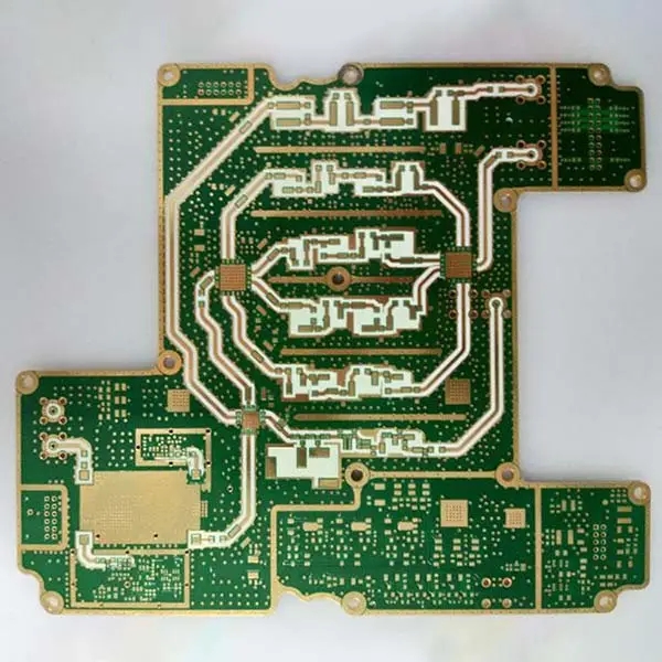
What is PCB differential signal? Generally speaking, the driver sends two equivalent and inverse signals, and the receiver judges whether the logic state is "0" or "1" by comparing the difference between the two voltages. The pair of wires carrying differential signals is called differential wiring.
Compared with ordinary single ended signal routing, differential signal has the most obvious advantages in the following three aspects:
a. Strong anti-interference capability, because the coupling between the two differential lines is very good, when there is noise interference from the outside, it is almost coupled to the two lines at the same time, and the receiver is only concerned about the difference between the two signals, so the external common mode noise can be completely offset.
b. It can effectively suppress EMI. In the same way, since the polarities of the two signals are opposite, the electromagnetic fields radiated by them can cancel each other. The tighter the coupling, the less electromagnetic energy released to the outside world.
c. The timing positioning is accurate. Because the switch change of differential signal is located at the intersection of two signals, unlike ordinary single ended signals, which are judged by high and low threshold voltages, it is less affected by process and temperature, which can reduce the timing error, and is more suitable for circuits with low amplitude signals. The current popular LVDS (low voltage differential signaling) refers to this small amplitude differential signal technology.
Why is PCB coated with copper?
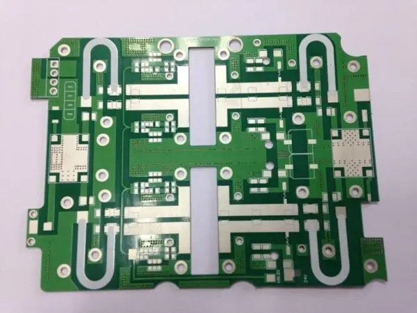
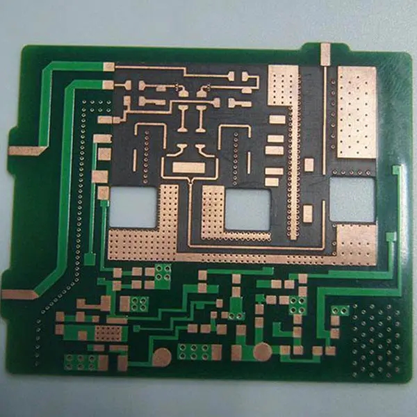
Copper covering refers to covering the area without wiring on the PCB with copper foil and connecting it with the ground wire to increase the area of the ground wire, reduce the area of the loop, reduce the voltage drop, and improve the power efficiency and anti-interference capability. In addition to reducing the ground wire impedance, copper coating can also reduce the loop cross-sectional area and enhance the signal mirror loop. Therefore, copper clad process plays a very important role in PCB process. Incomplete, truncated mirror loops or copper layers with incorrect positions often lead to new interference, which has a negative impact on the use of circuit boards.
DPC substrate preparation process
DPC substrate structure
Comparison between Copper Cladding Process and Thick Film Process
Project Copper Cladding Process Thick Film Process
The pure copper conductor, the metal component of the conductive circuit, has the advantages of excellent performance, not easy to be oxidized, and not producing chemical changes with time. The silver palladium alloy has the disadvantages of easy oxidation, easy migration and poor stability.
Bonding force of metal and ceramics The bonding force of PCB industry can reach 18-30 MPa. The bonding strength of Sliton ceramic circuit board is 45 MPa. The bonding force is strong, it will not fall off, and the physical performance is stable. The binding force is poor, which will be aging with the passage of application time, and the binding force is getting worse and worse.
The precision, surface flatness and stability of the line are etched. The line edge is neat without burrs, very fine, and has high precision. Sliton ceramic circuit board copper coating thickness is 1 μ Customized between m~1mm, line width and diameter can reach 20 μ m。 When printing is used, the product is relatively rough, and the edge of the printing line is easy to produce burrs and notches. The thickness of copper coating is 20 μ Below m, the minimum line width and diameter shall be 0.15 mm.
The line position accuracy uses the exposure development method, and the position accuracy is very high. The accuracy of screen printing will deviate with the increase of screen tension and printing times.
Line surface treatment Surface treatment process includes nickel plating, gold plating, silver plating, OSP, etc. Silver palladium alloy.
LAM process and DPC process
In LAM process, ceramic metallization uses high-energy laser beam to normalize ceramic and metal ions, so that they can be closely combined and grow together. The copper coating with LAM technology has the advantages of controllable copper layer thickness and easy control of graphic accuracy. The copper coating thickness of Siliton ceramic circuit board can be within 1 μ Customized between m~1mm, line width and line diameter can reach 20 μ m。 That is to say, with the application and deepening of science and technology in the laser field, the copper coating technology in PCB industry can achieve high bonding degree and excellent performance of ceramic and metal layers through laser technology.
In the DPC process, the electroplating process is adopted. Generally, the ceramic metallization uses the sputtering process to form an adhesive layer made of chromium or titanium and a seed layer made of copper on the ceramic surface in turn. The adhesive layer can increase the adhesion strength of the metal circuit, while the copper seed layer acts as a conductive layer. PCB manufacturers, PCB designers and PCBA manufacturers explain to you the advantages of differential wiring of PCB technology and why copper is covered on PCB?


Just upload Gerber files, BOM files and design files, and the KINGFORD team will provide a complete quotation within 24h.