
Professional PCB manufacturing and assembly
Building 6, Zone 3, Yuekang Road,Bao'an District, Shenzhen, China
+86-13410863085Mon.-Sat.08:00-20:00

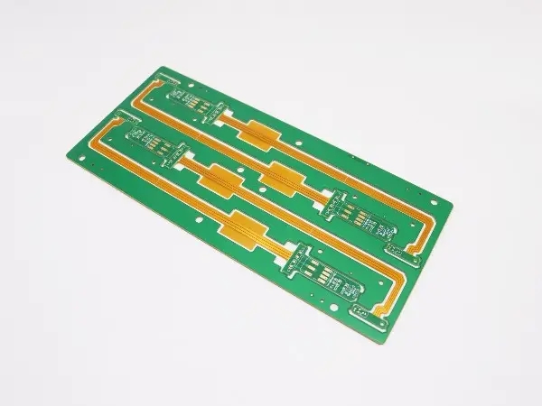
Methods of Copying Double Sided Board and Multilayer Board
Method for copying double-sided boards:
1. Scan the upper and lower layers of the PCB and save two BMP images.
2. Open the board copying software Quickpcb2005, click "File" and "Open base map" to open a scan image. Use PAGEUP to enlarge the screen, see the pad, press PP to place a pad, see the line and press PT to route... Just like a child's drawing, draw once in this software, and click "Save" to generate a B2P file.
3. Click "File" and "Open base map" again to open another layer of scanned color map;
4. Click "File" and "Open" again to open the previously saved B2P file. We can see that the board just copied is stacked on this picture - the same PCB board, the holes are in the same position, but the circuit connections are different. So we press "Options" - "Layer Settings", and turn off the display of lines and silk screen on the top layer here, leaving only multi-layer vias.
5. The vias on the top layer are at the same position as the vias on the picture on the bottom layer. Just as in childhood, just trace the lines on the bottom layer. Click "Save" again - the B2P file now has two layers of data: the top layer and the bottom layer.
6. Click "File" and "Export as PCB File" to get a PCB file with two layers of data. You can change the board again or issue the schematic diagram again or directly send it to the PCB plate making factory for production
Method for copying multilayer board:
In fact, the four layer board copying is to copy two double-sided boards repeatedly, and the six layer board copying is to copy three double-sided boards repeatedly... The reason why the multi layer board is so daunting is that we cannot see its internal wiring. How can we see the inside of a precision multilayer board—— layered.
There are many ways to solve the problem of layering, such as liquid medicine corrosion and tool stripping, but it is easy to divide the layer too much and lose data. Experience tells us that sandpaper grinding is the most accurate.
When we finish copying the top and bottom layers of PCB, we usually use sandpaper to polish the surface layer to show the inner layer; Sandpaper is a kind of ordinary sandpaper sold in hardware stores. Generally, the PCB is tiled, then the sandpaper is pressed and evenly rubbed on the PCB (if the board is very small, the sandpaper can also be tiled, and the PCB is pressed and rubbed on the sandpaper with a finger). The key point is to pave it so that it can be ground evenly.
The silk screen and green oil are usually wiped off, and the copper wire and copper skin should be wiped well. Generally speaking, the Bluetooth board can be wiped in a few minutes, and the memory module takes about ten minutes; Of course, with great strength, it will take less time; It will take a little more time.
Grinding plate is the most commonly used scheme for layering at present, and it is also the most economical. We can find an abandoned PCB to try. In fact, there is no technical difficulty in grinding the board, but it is a little boring. It takes some effort, and you don't have to worry about wearing the board to your fingers.
PCB manufacturers, PCB designers and PCBA processors will explain the methods of double-sided board copying and multilayer board copying.


Just upload Gerber files, BOM files and design files, and the KINGFORD team will provide a complete quotation within 24h.