
Professional PCB manufacturing and assembly
Building 6, Zone 3, Yuekang Road,Bao'an District, Shenzhen, China
+86-13410863085Mon.-Sat.08:00-20:00


Last article Xiao bian and everyone together to understand the electronic components on the circuit board, how do you harvest. So how does a circuit board work? How does it work? This article will continue with you to learn more about circuit boards.
A circuit board may be called a printed circuit board or printed circuit board, (Printed Circuit Board)PCB (Flexible Circuit Board) FPC Circuit Board (FPC Circuit Board) FPC Circuit Board (FPC Circuit Board) Flexible Circuit Board is made of polyimide or polyester film as the base material, providing high reliability. Excellent flexible printed circuit boards. The name of the circuit board is: ceramic circuit board, alumina ceramic circuit board, aluminum nitride ceramic circuit board, circuit board, PCB board, aluminum substrate, high-frequency board, thick copper plate, impedance board, PCB, ultra-thin circuit board, ultra-thin circuit board, printing (copper etching technology) circuit board and so on.

The working principle of
The working principle of the circuit board is to use the plate base insulation material to separate the surface copper foil conductive layer, so that the current flows along the pre-designed route in various components to complete functions such as doing work, amplification, attenuation, modulation, demodulation, coding and so on.
composition
The circuit board is mainly composed of solder pads, holes, mounting holes, wires, components and connectors. The thin-film circuit of Waterford circuit board SMT SMT, filling, electrical boundary, etc. The main functions of each component are as follows:
Pad: A metal hole used to weld the pin of a component.
Through: There are metal through holes and non-metal through holes, where metal through holes are used to connect component pins between layers.
Mounting hole: used to secure the circuit board.
Wire: Copper film of electrical network used to connect pin of component.
Connector: A component used to connect circuit boards.
Padding: Copper coating for grounding networks, which effectively reduces impedance.
Electrical boundary: Used to determine the size of the circuit board. No component on the circuit board should exceed this boundary.
FIG. 2 Hole structure of circuit board
classification
Circuit board according to the number of layers to be divided into single panel, double panel, and multilayer circuit board three major categories.
Multilayer board: a printed board with more than three conductive pattern layers and insulation materials in between layers laminated separately, and the conductive pattern in between layers interconnected as required. Multilayer circuit board is the electronic information technology to high speed, multi-function, large capacity, small volume, thin, lightweight direction of the development of the product.
Single panel: On the most basic PCB, the parts are concentrated on one side and the wires are concentrated on the other. Because the wires appear on only one side, the PCB is called a single-sided circuit board. Single panels are usually simple and inexpensive to make, but have the disadvantage that they cannot be applied to too complex products.
Double panel: is the extension of the single panel, when the single layer wiring can not meet the needs of electronic products, it is necessary to use the double panel. Both sides are covered with copper wires, and the wires between the two layers can be guided through holes to form the required network connection.
According to the characteristics of the circuit board is divided into soft board (FPC), hard board (PCB), soft and hard board (FPCB).
Figure 3 Multilayer circuit board
The work level
The circuit board includes many types of working layers, such as signal layer, protective layer, screen printing layer, internal layer, etc. The roles of each layer are briefly described as follows:

(1) Protective layer: mainly used to ensure that the circuit board does not need tin plating place is not tin plating, so as to ensure the reliability of the circuit board operation. The Top Paste and Bottom Paste are the Top welding resistance layer and the Bottom welding resistance layer respectively. Top Solder and Bottom Solder are Solder coating and Bottom Solder coating, respectively.
(2) Signal layer: mainly used for placing components or wiring. Protel DXP usually contains 30 intermediate layers, namely Mid Layer1~Mid Layer30. The middle layer is used to arrange signal cables, while the top and bottom layers are used to place components or apply copper.
(3) Screen printing layer: it is mainly used to print the serial number, production number and company name of components on the circuit board.
(4) Internal layer: mainly used as signal wiring layer, ProtelDXP contains a total of 16 internal layers.
(5) Other layers: It mainly includes four types of layers.
Drill Guide(Drill bearing layer) : mainly used for Drill position on printed circuit board.
Keep-out Layer: used to draw the electrical border of the circuit board.
Mainly used for setting the shape of drilling holes.
Multi-layer: Sets the multi-layer Layer.
Figure 4 Working level of circuit board
This paper introduces the concept, working principle, composition, classification and working level of circuit board. Depending on the design of the circuit board, the price will be determined by the material of the circuit board, the number of layers of the circuit board, the size of the circuit board, the quantity of each production, the production process, the minimum line width and line distance, the minimum aperture and the number of holes, the special process and so on.
Beijing First Silicon Core Technology has been engaged in chip decryption for many years, involving business including PCB copying board, MCU development, chip decryption, encryption algorithm research, chip burning services, etc. PCB board copying service can provide PCB reverse schematic diagram, BOM list, PCB board modification, chip decryption and other comprehensive services. If you have any needs, please contact us directly.
What is the meaning of a circuit board?
Oct 30,2022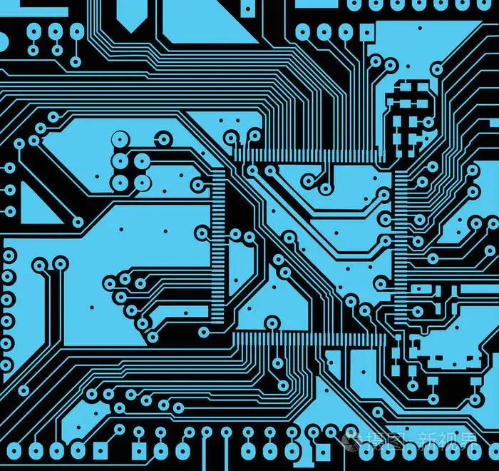


Just upload Gerber files, BOM files and design files, and the KINGFORD team will provide a complete quotation within 24h.