
Professional PCB manufacturing and assembly
Building 6, Zone 3, Yuekang Road,Bao'an District, Shenzhen, China
+86-13410863085Mon.-Sat.08:00-20:00

High-density PCB board is a structural component formed by insulating material supplemented with conductor wiring. Electrical signals and functions can be formed through wire connection. Therefore, a high-density PCB is a platform that provides component connectivity and is used to carry the foundation of the connected parts.

1 High density PCB board development process
Because printed circuit board is not a general end product, so in the name of the definition of a slightly confused, for example: personal computer motherboard, called the host board and not directly called the circuit board, although there is a circuit board in the host board but not the same, so the assessment of the industry when the two related but can not say the same. Another example: because there are integrated circuit parts loaded on the circuit board, so the news media called it IC board, but in essence it is not equivalent to printed circuit board. As electronic products tend to be multifunctional and complex, the contact distance of integrated circuit components is reduced, and the speed of signal transmission is relatively increased, followed by the increase of the number of connections and the local shortening of the length of distribution lines between points. These require the application of high-density line configuration and micropore technology to achieve the goal. Wiring and bonding are basically difficult to achieve for single and double panels, so the Circuit Board will move to Multilayer. In addition, due to the continuous increase of signal lines, more power layers and grounding layers are necessary means for design, which makes the Multilayer Printed Circuit Board more common.
2 Advantages of high-density PCB board
For the electrical requirements of high speed signals, the circuit board must provide impedance control with alternating current characteristics, high frequency transmission capability, and reduction of unnecessary radiation (emi). With Stripline and Microstrip structure, multilevel design becomes necessary. To reduce quality problems in signal transmission, insulation materials WITH low dielectric coefficient and low attenuation rate are used. In order to match the miniaturization and array of electronic components, the density of circuit boards is constantly increased to meet the demand. BGA (Ball Grid Array), CSP (Chip Scale Package), DCA (Direct Chip Attachment) and other groups of parts assembly, more promote the printed circuit board to an unprecedented high density realm. Where the diameter of the hole less than 150um is known as Microvia in the industry, the use of this microhole geometry technology to make the circuit can improve the efficiency of assembly, space utilization and so on, at the same time for the miniaturization of electronic products also has its necessity. For this type of structure of the circuit board product, the industry has a number of different names to call such a circuit board. For example, European and American companies used to call such products SBU (Sequence Build Up Process), which is generally translated as "sequential layer adding method", because the programs they made were constructed in a sequential way. As for the Japanese manufacturers, because the hole structure of these products is much smaller than the previous ones, the production technology of these products is called MVP (Micro Via Process), which is generally translated as "Micro hole Process". Some people because the traditional Multilayer Board is called MLB (Multilayer Board), so this kind of circuit Board is called BUM (Build Up Multilayer Board), generally translated as "layered Multilayer Board".
3 High-density PCB Name
In order to avoid confusion, the American IPC Circuit Board Association proposed to call such products the generic name of High Density Intrerconnection Technology (HDI), which translates directly into High Density connection Technology. However, this does not reflect the characteristics of the board, so most circuit board manufacturers refer to such products as HDI board or the full Chinese name "high density interconnect technology". However, some people refer to such products as "high-density circuit boards" or HDI boards because of the problem of smooth speaking.

4. Design challenges of high-density PCB board
With the increasingly high volume requirements of information products, especially the development of mobile device products in the direction of continuous miniaturization, such as the current hot Ultra Book products, or even novel wearable intelligent devices, must use HDI high-density interconnect technology to make the carrier board, which further reduces the size of the terminal design. High Density Interconnect (HDI) refers to the High Density Interconnect technology, which is one of the technologies used by the Printed circuit Board (PCB). HDI mainly micro buried blind hole technology was used to make, features can make printed circuit boards in electronic circuit distribution line density is higher, and the power density, also let HDI made of printed circuit board can't use general way into a hole drilling, HDI must adopt the mechanical drilling process, the method of mechanical drilling is quite much, Among them, "laser hole formation" is mainly the collocation hole formation scheme of HDI high-density interconnect technology. HDI printed circuit boards are widely used in mobile phones, ultra-thin laptops, tablet computers, digital cameras, automotive electronics, digital cameras... Electronic products, such as HDI technology has been used to reduce the motherboard design, reduced the benefit is considerable, not only the end product design can leave more space for batteries, or more additional function components, the cost of products can also be relatively reduced because of the import of HDI. HDI was used in the early stage of medium and high price mobile phones, and now it is almost popular in the early stage of all mobile devices that use the most HDI technology, mainly feature phones and smart phones. Such products account for more than half of the consumption of HDI high-density circuit boards, while any-layer HDI(high-density connection board of Any layer) is the manufacturing process of high-order HDI. The biggest difference with the general HDI circuit board is that most HDI is carried out by the drilling process of the PCB through the machine drill, as for the layer between the sheet, Any-layer HDI uses "laser" drilling to open up each layer of the interconnectivity design. For example, the production method of Any-Layer HDI can generally reduce the volume of PCB by about 40%. At present, Any-Layer HDI has been used in Apple iPhone 4.
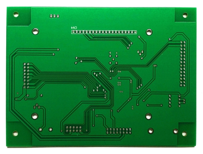
This is a high-density circuit board.
What is a circuit board?
Oct 29,2022


Just upload Gerber files, BOM files and design files, and the KINGFORD team will provide a complete quotation within 24h.