
Professional PCB manufacturing and assembly
Building 6, Zone 3, Yuekang Road,Bao'an District, Shenzhen, China
+86-13410863085Mon.-Sat.08:00-20:00

The rapid development of PCB industry and the increasing demand for PCB (printed circuit board) manufacturing industry, including rising circuit board layers, higher tracking density and thinner inner layers, all of which lead to the increasing importance of lamination and lamination technology.
In order to prevent quality problems in the stacking process, such as dislocation, fusion is usually required before stacking in the multi-layer process. Compared with traditional fusion technology, modern fusion technology has the advantages of high efficiency, easy operation, low cost, etc., which makes it easy to make multi-layer PCB. Starting from the basic technology of fused PCB manufacturing, this paper discusses the parameter factors that affect the fusion effect and the application level of fusion technology, so as to provide a reliable reference for obtaining the best fusion parameters.
Principle fusion technology
As a traditional technology, rivet technology has been widely used in PCB manufacturing. However, rivet technology also has some disadvantages, such as high rivet cost, dislocation caused by PCB deformation, easily damaged template, rivet shape indentation on PCB, etc., and high PCB cost. Therefore, fusion technology has been continuously used to replace rivet technology.
Introduction to PCB Rivet Technology
According to the melting characteristics of the epoxy resin prepreg, the melting technology can make the prepreg melt at a certain temperature, thus converting the B-phase epoxy resin into the C-phase epoxy resin, and the inner layer is connected by the adhesive. Fusion is one of the most important processes in the laminating process, and its performance directly determines the laminating behavior. The key elements of integration technology include:
• Accuracy of positioning system
The type of positioning system is directly related to the alignment accuracy, which further affects the percentage of passing rate. An excellent positioning system should be stable, reliable and repeatable.
• Fusion point design
Fusion points are an essential issue because fusion techniques involve many shapes, such as square, round and oval. The fusion points should be consistent in area, because fusion points with too small area tend to lead to weak fusion welding, while fusion points with too large area tend to lead to image penetration, which may lead to loose connection between white spots, inner layers or
• Equipment flatness
The flatness of the equipment will affect the angle of PCB in the fusion process, the force distribution and time balance in the fusion process. The non-uniformity will lead to the deformation of the circuit board, which will further lead to the dislocation between layers.
• Temperature and time control
During the implementation of fusion technology, the temperature and time shall be carefully controlled to avoid burning, white spots, desoldering and aging. In addition, the stack of PCB also plays an important role in determining the fusion effect.
Factors Affecting Fusion Performance in FusionPCB Manufacturing
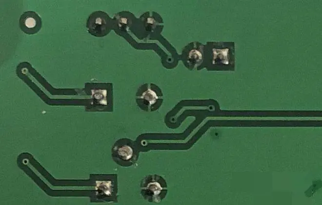
PCB fusion welding joint
Different fusion and fusion effects are summarized in the following table, which is applicable to different types of fusion welded joints.
Based on the above table, since the area of rectangular fusion welded joint is twice as large as that of circular fusion welded joint, the adhesion produced by rectangular fusion welded joint is significantly greater than that produced by circular fusion welded joint. However, the resin flow generated by rectangular fusion welded joints is far greater than that generated by circular fusion welded joints. When the resin flow is too large, some plate sides may be higher than the plate, which may lead to virtual pressure on the plate side. For small size PCB products, due to the limited melting point that can be designed and the small area of circular fusion welding joints, the fusion effect is insufficient. Therefore, rectangular fusion welded joints should be selected and the fusion position should be carefully designed. As the plate moves inward, the defect of resin overflow can be eliminated.
• Melting temperature
When the melting temperature reaches 300 ° C, the fusion expansion area is large, and the polymerization effect is seriously affected. When the melting temperature reaches 270 ℃, the fusion expansion area is uneven, and the risk of cracks is high, resulting in fusion effect. When the melting temperature reaches 285 ℃, the fusion expansion is uniform and there is no risk of cracks, leading to the best fusion effect. Therefore, it can be concluded that 285 ° C is the best melting temperature for multi-layer PCB manufacturing at the same melting time and stacking.
• Melting time
At the equivalent melting temperature and lamination, different fusion time will affect the fusion extension region and fusion effect. When the melting time is 12 seconds, the fusion expansion area is uneven, with the risk of cracks and poor fusion effect. When the fusion time is 18 seconds, the fusion expansion area is large and the fusion effect is poor. When the fusion time is 15 seconds, the fusion expansion is uniform, without crack risk and optimal fusion effect. Therefore, at the equivalent melting temperature and equivalent layer stacking, 15 seconds is the best fusion time for multi-layer PCB manufacturing. If the fusion time is too long or too short, it will bring bad fusion effect.
• PCB stacking
Equivalent fusion temperature and fusion time, different layers determine the fusion region and fusion effect. Under the equivalent melting time and temperature, when the prepreg 2116 is applied, there is no crack in the fusion expansion area, leading to the best fusion effect. At the equivalent melting time and temperature, when the prepreg 7628 is applied, the fusion expansion area even has cracks. This shows that at the same melting time and temperature, the thinner the prepreg is, the better the fusion effect will be. Therefore, it can be concluded that the layers of 2116 prepreg or lower layers are suitable for the realization of melting technology in the manufacturing process of multilayer PCB.
According to the discussion in this paper, there are many factors that affect the fusion effect: the shape of fusion welded joint, melting temperature, fusion time and lamination. Rectangular fusion welded joint has better fusion effect than circular fusion welded joint. When the equivalent layers are superposed and fused, the higher the fusion temperature, the larger the fusion expansion area. If the melting temperature is too low, the fusion expansion area will be uneven and there is a risk of cracks. The longer the fusion time is, the larger the fusion expansion area is. When the fusion time exceeds 15 seconds, the fusion expansion area will expand, resulting in adverse fusion effects. The thinner the prepreg blank structure is, the more uniform the melt expansion is. Therefore, 2116 or lower prepreg is most suitable for fusion.


Just upload Gerber files, BOM files and design files, and the KINGFORD team will provide a complete quotation within 24h.