
Professional PCB manufacturing and assembly
Building 6, Zone 3, Yuekang Road,Bao'an District, Shenzhen, China
+86-13410863085Mon.-Sat.08:00-20:00

In PCB industry, almost all electrical products will use circuit boards, which is an indispensable electronic component and the heart of all electrical appliances. The following Fanyi Circuit introduces the process of electronic circuit board, and I hope it will be helpful to you!
Circuit board production
1. Evaluation of engineering data of pcb circuit board: the customer places an order online, automatically reviews and quotes through the independently developed IPCB CAM software, and automatically opens materials for production in connection with the factory.
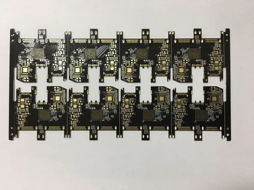
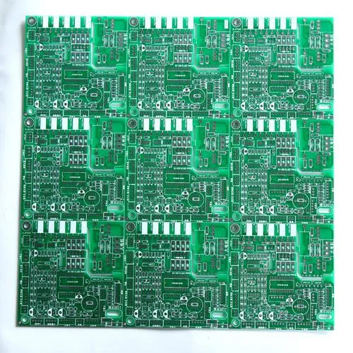
2. Preparation for material opening: Three domestic plates are used: Guoji, Jiantao and Shengyi (select one according to the customer's requirements). These plates are all mechanically and accurately cut. Good products are made from the source. Shenzhen Qinji Electronics uses these plates.
3. Drilling: The imported precision high-speed drilling rig is used to rapidly complete a large number of drilling operations in a short time.
4. Copper sinking: the manufacturer uses automatic copper sinking wire operation to reduce manual practices and improve quality stability. Professional operators monitor the concentration of I to be delivered in real time to ensure production.
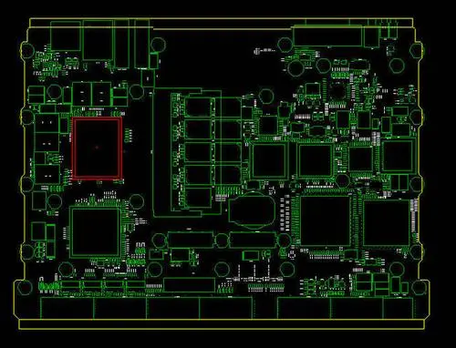
5. Graphic transfer: adopt imported film pressing machine and dry film production, pin pin alignment, to ensure the line diameter class and line spacing.
6. Electroplating: adopt chemical production, thicken the hole copper grade surface to ensure the optimal electrical performance of pcb board.
7. AOI optical detection: quality inspection before candle engraving, to ensure one-time pass rate, using foreign well-known imported equipment.
8. Convert the customer's original documents into film negatives, and package them after inspection to prepare for the graphic transfer of the subsequent process.
9. Silk screen printing text: The full-automatic text silk screen printing machine is used to ensure the clarity and stereoscopic sense of the text and facilitate SMT welding.
10. Surface treatment: the general surface treatment of PCB factory includes lead tin spraying, lead-free tin spraying, gold deposition, OSP oxidation resistance, gold plating, tin deposition, silver deposition, nickel deposition, bare copper and chemical separation plate.
11. CNC molding: high-precision CNC is introduced to ensure the tolerance level appearance of PCB board dimensions, and improve production efficiency (large quantities require mold opening).
12. Final inspection and test of circuit board: this step is the end of the production line. All of them use the high-speed flying probe tester level special test stand tester. The high-speed tester is also the equipment provided by most PCB manufacturers at present, which is expensive, and the efficiency of nitrogen detection is unmatched by ordinary equipment.


Just upload Gerber files, BOM files and design files, and the KINGFORD team will provide a complete quotation within 24h.