
Professional PCB manufacturing and assembly
Building 6, Zone 3, Yuekang Road,Bao'an District, Shenzhen, China
+86-13410863085Mon.-Sat.08:00-20:00

Some STM32 application customers who use external SDRAM reported that the radiated interference of their products exceeded the standard due to SDRAM signals during EMC testing. If the enclosure cannot be used to shield the radiated interference in terminal PCB products, such problems often need to be solved by modifying the PCB design of SDRAM signals.
Here is an overview of how to improve the radiated interference problem in the PCB application design of SDRAM for reference.
SDRAM Radiation Interference Countermeasure in Design
SDRAM works at a high frequency and has steep rising and falling edges. Therefore, it is necessary to process its signal routing as a high-speed signal transmission line in PCB design. In general, the following basic principles should be noted:
1. Keep SDRAM signal integrity
The distortion of SDRAM signal will further broaden the radiation spectrum of the signal, resulting in more serious radiation problems. Therefore, attention must be paid to the integrity design of SDRAM signal when outsourcing PCB design.
It is recommended to use four or more layers of boards to control the characteristic impedance of SDRAM signal at 50 ohms, minimize the use of vias on SDRAM bus, maintain impedance continuity, and reduce signal reflection caused by impedance discontinuity;
The SDRAM signal wiring spacing shall follow the principle of 3W, and the spacing between two wiring centers shall be kept at least 3 times of the line width as far as possible, which can reduce the signal distortion caused by the interference between signals;
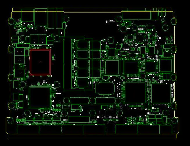
Keep SDRAM close to MCU as much as possible, and shorten the length of signal wiring from MCU to SDRAM (generally not more than 120mm);
2. Keep the shortest SDRAM signal return path
For multilayer PCB, the return path of high-speed signal is the projection of its routing on the reference plane. In PCB design, attention should be paid to maintaining the integrity and continuity of its reference plane. If the signal return path is cut off due to signal layer change or power supply layer division, the shortest return path of SDRAM signal must be ensured by adding layer change capacitance/layer change ground via and power supply plane jumper capacitance.
3. Place SDRAM signal (especially clock signal) on the inner layer of PCB
Among SDRAM signals, the clock signal has the strongest radiation level, which can be reduced by laying it on the inner layer of PCB and shielding it with outer copper foil.
The FMC interface of STM32 is designed with SDRAM and FLASH attached at the same time. Because SDRAM and FLASH share some MCU pins, their complex routing topology further enhances the radiation interference of SDRAM signals. It is recommended that SDRAM and FLASH routing be laid on the inner layer of PCB as much as possible, and these signals are shielded on the outer layer of PCB at the same time.
4. Keep SDRAM cabling area as far away from other signals/cables as possible
Long other routing lines or cables can be used as antennas to send out the coupled SDRAM radiation signals, so they should be arranged in the area far away from SDRAM signals in the PCB. When necessary, magnetic beads or filters can be placed at the connection ends of these routing lines or cables to attenuate SDRAM radiation signals.


Just upload Gerber files, BOM files and design files, and the KINGFORD team will provide a complete quotation within 24h.