
Professional PCB manufacturing and assembly
Building 6, Zone 3, Yuekang Road,Bao'an District, Shenzhen, China
+86-13410863085Mon.-Sat.08:00-20:00

After importing design data, the design engineer will start PCB layout design. The layout often determines the success or failure of the board. What are the layout problems we encountered in those years? After the layout is completed, there is no space for punching? The extra filter capacitor is placed around the BGA, and the power supply is crossed. How painful?
It is always difficult to connect, and there will always be a croshigh-speed PCBs, and the layout needs to be adjusted again.
First, rapid modularization
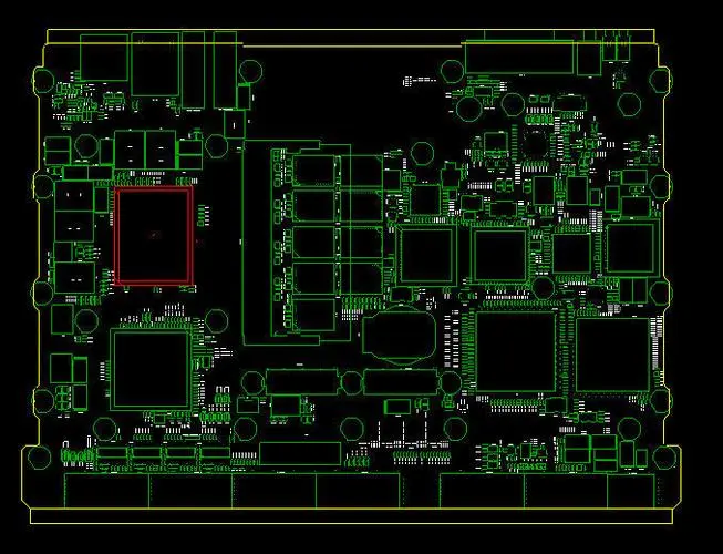
Modularization is a commonly used method for layout. Layout small functional modules according to the schematic diagram before overall layout in the board
The identified modules can be prioritized, such as DDR, power module, etc., or reused on other boards
Modules should be made into regular shapes, such as square or rectangle (conducive to layout, later adjustment, and even adjustment of revised design)
Consider the module as a whole, and clarify its input and output
Have an overall grasp of the size of modules, and make full use of the space between modules
Distinguish between primary and secondary, and consider in advance where special treatment is required
Second, partition layout
Third, overall pre layout
Key point: we need to have an overall grasp of the board and find a direction
The overall pre layout is not limited by the size of the board frame, and DRC can be ignored. After the modules are completed, you should have a general understanding of each module. In the pre layout adjustment process, you should know which one belongs to the power supply, which one is DDR, and which one is interface, without looking at the schematic diagram
Fourth, modular layout
1. Power supply
Whether the power supply is stable and reliable is one of the key factors for the success of PCB product design.
Firstly, the power flow direction of the whole board should be clarified, and the power input socket should usually be set at the corner of the board.
Next, pre layout each switching power conversion module.
Need to clarify:
Input, output, ground, sampling or feedback.
Switch power supply pre distribution
First, pre layout according to datasheet recommendations or schematic diagrams,
Then compress the space according to the specific situation.
Plan PCB wiring channel in advance by Fanout
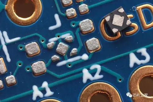
BGA filter capacitor placement:
Placed from inside to outside
Swing the cross channel first, then other PLL power supplies
Large capacitors are evenly placed around or on the power channel
The extra capacitance is placed around the BGA.
Fifth, PCB layout optimization
Start to optimize and adjust after clearing the direction
On a single PCB board with plenty of space, we usually have finished the module and can put it into the board frame. However, when making high-density boards, I found that there was not enough space for the finished modules to be placed. There were always conflicts in some places and I had to readjust them. Sometimes, I would repeat a lot of useless work. When optimizing modules and blocks, we should first evaluate whether they can be put into the predetermined area to optimize the module layout principle: estimate the space and allocate it reasonably.


Just upload Gerber files, BOM files and design files, and the KINGFORD team will provide a complete quotation within 24h.