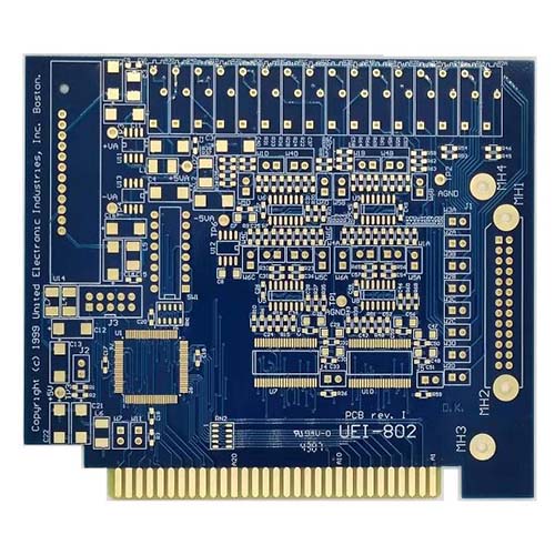
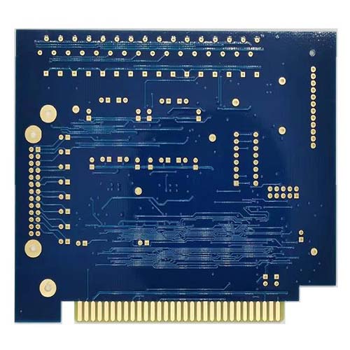
Double-sided gold finger circuit board
Name: Double-sided gold finger circuit board
Plate: FR4
Layers: 2L
Material: S1141
Plate thickness: 1.6mm
Copper thickness of inner and outer layers: 1oz
Minimum aperture: 0.3mm
Surface Treatment: Immersion Gold
Line width: 0.15mm
Line distance: 0.15mm
Others: electroplating gold fingers
Blind hole structure: L1-L2
Use: board, interface
Gold-finger PCBs are those with gold-finished finger-like pads that are typically used as edge connectors.
Electroless gold has excellent solderability, but the chemical deposition process means it is too soft and thin to withstand repeated wear and tear. Gold plating is thicker and harder, making it ideal for re-mating PCB edge connector contacts.
Gold finger PCBs often have to be chamfered at the edge connectors to ensure easy insertion. Bevel cuts can be specified in the order details if specifically stated.
Gold fingers are the gold-plated posts you see on the edge of a printed circuit board (PCB) connection. The purpose of the golden finger is to connect the auxiliary PCB to the motherboard of the computer. PCB gold fingers are also used in various other devices that communicate via digital signals, such as consumer smartphones and smart watches. Gold is used for connection points along the PCB due to the alloy's excellent electrical conductivity.
There are two kinds of gold suitable for PCB gold finger plating process:
Electroless Nickel Immersion Gold (ENIG): This gold is more cost-effective and easier to solder than electroplated gold, but its soft, thin (typically 2-5u” composition makes ENIG unsuitable for circuit board insertion and removal wear and tear Effect.
Electroplated hard gold: This gold is solid (hard) and thick (usually 30u”), so it is more suitable for the abrasive effects of continuous use of the PCB.
Gold fingers enable different circuit boards to communicate with each other. From a power source to a device or equipment, a signal must pass between multiple contacts in order to execute a given command.
When a command is pressed, the signal is passed between one or more boards before being read. For example, if you press a remote command on your mobile device, a signal will be sent from the PCB-enabled device in your hand to a nearby or distant machine, which in turn will receive the signal through its own circuit board.
The process of gilding fingers involves many meticulous steps. This ensures that every circuit board that rolls off the production line is equipped with the correct equipment to conduct the signal flawlessly. The standards involved in the plating process also help ensure that the gold fingers on each circuit board match perfectly with the corresponding sockets on a given motherboard.
To ensure that all of these fingers and sockets fit in the hand in the glove, each PCB must pass a series of inspections and defect tests. If the gold plating on the board lacks smoothness or does not adhere sufficiently to the surface, the results will not be sufficient for commercial release.
In order for the PCB gold fingers to come together, the electroplating process must take place in a step that first completes the details around the board. When it is time to plate the fingers, nickel is applied to the copper. Then, finally apply the surface finish. When everything is in place, inspect the board under a magnifying glass and do an adhesion test.
During PCB gold finger plating, certain standards must be followed for the fingers to function properly. The design of the PCB itself must also take into account the area required for proper finger length and alignment. Regardless of the purpose or size of the PCB itself, the following rules always apply to the design of gold fingers:
Plated through holes should not be close to gold fingers.
The gold fingers should not have any contact with the solder mask or silk screen, and the two should be kept at a certain distance.
Gold fingers must always face opposite the middle of the PCB (if you want the edge beveled)
If any of these rules are not followed during PCB gold finger plating, the PCB may not be able to communicate with the mother circuit board. Alternatively, the PCB may not fit properly into the corresponding slot on the motherboard.
Gold is used for the connection fingers on the PCB because of the alloy's excellent strength and electrical conductivity. The strength of the gold allows fingers to be inserted and ejected hundreds of times without fraying the connecting contacts. Without the protection of gold plating, the board can easily lose connectivity after a few uses.
You may be wondering why gold is better than other types of metals. After all, gold is one of the rarest and most expensive natural elements. Is it more cost effective to plate the connection edges of the PCB with copper or nickel? However, gold is required for the desired function of the printed circuit board.
As PCBs evolved into their modern form, gold was determined to be the most suitable connection contact metal due to a number of factors. The main advantages of gold are the electrical conductivity and corrosion resistance of the alloy. For added strength, gold used in printed circuit boards is often combined with nickel or cobalt, which gives gold further wear resistance in the face of constant PCB activity. For the electroplating process, the thickness of nickel is between 150 and 200 microinches.
The production standard for PCB gold fingers was established in 2002 by the Connected Electronics Industry Association (IPC). These standards were revised in 2012 with the publication of IPC-4556. In 2015, these standards were revised again with the publication of IPC A-600 and IPC-6010, which are currently the most widely used standards in PCB production. The IPC standards can be summarized as follows:
Chemical composition: For maximum rigidity at the edges of the PCB contacts, the gold plating layer should contain 5% to 10% cobalt.
Thickness: Gold finger plating thickness should always be in the range of 2 to 50 microinches. Standard thicknesses by size are 0.031", 0.062", 0.093" and 0.125". Lower thicknesses are typically used for prototypes, while higher thicknesses are used along connecting edges that are regularly inserted, unplugged, and reinserted.
Visual test: The visual test that the golden finger should be conducted through a magnifying glass. The edges should have a smooth, clean surface with no unwanted plating or the appearance of nickel.
Tape Test: To test the adhesion of gold plating to contacts, ICP recommends testing by placing a strip of tape along the edge of the contact. After removing the tape, inspect the tape for traces of plating. If there is significant gold plating on the tape, the plating lacks sufficient adhesion with the contacts.
Name: Double-sided gold finger circuit board
Plate: FR4
Layers: 2L
Material: S1141
Plate thickness: 1.6mm
Copper thickness of inner and outer layers: 1oz
Minimum aperture: 0.3mm
Surface Treatment: Immersion Gold
Line width: 0.15mm
Line distance: 0.15mm
Others: electroplating gold fingers
Blind hole structure: L1-L2
Use: board, interface
- Previous:Double-sided industrial control PCB board
- Next:No