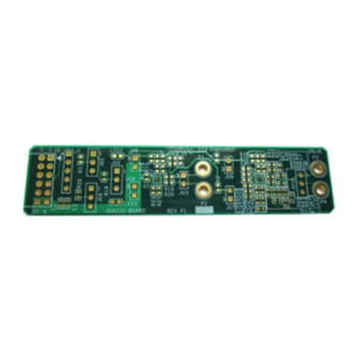
Small BGA Rigid Printed Circuit Boards
Name: Small BGA circuit board PCB
Layers: 4 layers
PCB Material: FR4 TG170
PCB thickness: 1.6mm
Surface treatment: Immersion Gold ENIG(Gold thickness 2u”)
Finished Copper Thickness: 1/1/1/1 OZ
Solder Mask Ink: Green, Sun PSR-4000
Special Process:
Minimum line width and line spacing: 0.07/0.09mm
BGA pad: 0.25 mm
The full name of BGA is Ball Grid Array (PCB with ball grid array structure), which is a pin packaging method for large components. The difference is the "one-degree space" single-row pins listed around, such as gull-wing extension feet, flat extension feet, or J-shaped feet retracted to the abdominal bottom, etc.; change to a full array or partial array of the abdominal bottom, The distribution of solder balls with two-dimensional space area is adopted as a welding and interconnection tool for the chip package to the circuit board. It has the characteristics of small package area, increased function, increased number of pins, high reliability, good electrical performance and low overall cost.
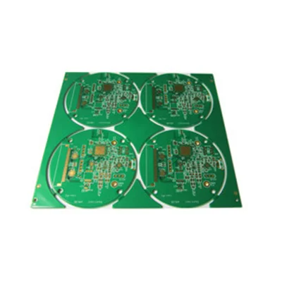
Name: Small BGA circuit board PCB
Layers: 4 layers
PCB Material: FR4 TG170
PCB thickness: 1.6mm
Surface treatment: Immersion Gold ENIG(Gold thickness 2u”)
Finished Copper Thickness: 1/1/1/1 OZ
Solder Mask Ink: Green, Sun PSR-4000
Special Process:
Minimum line width and line spacing: 0.07/0.09mm
BGA pad: 0.25 mm