

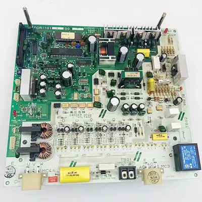
Multilayer PCBA Board Copy Clone
Name: Multilayer PCBA Board Copy Clone
Layers: 1-32 layers
Minimum line width and line spacing: 3mil
Minimum laser aperture: 4mil
Minimum mechanical aperture: 8mil
Copper foil thickness: 18-175цm (standard: 18цm35цm70цm)
Peel strength: 1.25N/mm
Minimum punching hole diameter: single side: 0.9mm/35mil
Minimum hole diameter: 0.25mm/10mil
Aperture tolerance: ≤φ0.8mm±0.05mm
Hole tolerance: ±0.05mm
Hole wall copper thickness: double-sided/multi-layer: ≥2um/0.8mil
Hole resistance: double-sided/multi-layer: ≤300цΩ
Minimum line width: 0.127mm/5mil
Minimum pitch: 0.127mm/5mil
Surface treatment: rosin spray tin electric gold, anti-oxidation, chemical gold, carbon oil
Warpage: ≤0.7%
A multilayer PCB is a circuit board with more than two layers. Unlike double-sided PCBs, which have only two layers of conductive material, all multilayer PCBs must have at least three layers of conductive material buried in the center of the material.
As the name suggests, a multilayer PCB is a combination of different layers. A single-sided PCB and a double-sided PCB combine to form a PCB of this complex design. Multilayer PCBs increase the number of layers and therefore increase the area available for routing. These boards are made by combining two-layer PCBs and separating them with insulating materials such as dielectrics.
Conductive layers between insulating materials are a minimum of three, and we can incorporate up to a hundred layers as needed. We treat multilayer PCBs as rigid PCBs because it is difficult to manufacture flexible multilayer PCBs. Most of our common multilayer PCBs consist of 4 to 8 layers. Smartphones can contain up to 12 layers as they suit the complexity of the application. Manufacturers prefer even-numbered layers to odd-numbered layers, because laminating odd-numbered layers can make the circuit overly complex and problematic, and high cost is also a factor to consider.
Multilayer PCBs have some advantages over single or double layer PCBs. They have higher densities, allowing for greater functionality, capacity and speed. Electromagnetic shielding is easier if the power and ground planes are placed correctly. No extensive wiring is required, so it is lightweight. They reduce size and help save space. They are more flexible than other types of PCBs.
Multilayer PCBs have many applications. These include:
· computer
· Fiber optic receiver
· data storage
· Signal transmission
· Mobile phone transmission
· Cell Phone Repeater
· GPS technology
· industrial control
· Satellite system
· Handheld devices
· Test equipment
· X-ray equipment
· Heart monitor
· Cat scanning technology
· Atomic accelerator
· Central fire alarm system
· Fiber optic receiver
· Nuclear detection system
· Space detection equipment
· Weather analysis
Name: Multilayer PCBA Board Copy Clone
Layers: 1-32 layers
Minimum line width and line spacing: 3mil
Minimum laser aperture: 4mil
Minimum mechanical aperture: 8mil
Copper foil thickness: 18-175цm (standard: 18цm35цm70цm)
Peel strength: 1.25N/mm
Minimum punching hole diameter: single side: 0.9mm/35mil
Minimum hole diameter: 0.25mm/10mil
Aperture tolerance: ≤φ0.8mm±0.05mm
Hole tolerance: ±0.05mm
Hole wall copper thickness: double-sided/multi-layer: ≥2um/0.8mil
Hole resistance: double-sided/multi-layer: ≤300цΩ
Minimum line width: 0.127mm/5mil
Minimum pitch: 0.127mm/5mil
Surface treatment: rosin spray tin electric gold, anti-oxidation, chemical gold, carbon oil
Warpage: ≤0.7%
