
Professional PCB manufacturing and assembly
Building 6, Zone 3, Yuekang Road,Bao'an District, Shenzhen, China
+86-13410863085Mon.-Sat.08:00-20:00

Chips are what we call ICs, which are composed of crystal elements and external packages. As small as a triode, our computer CPUs are all what we call ICs. Generally, they are installed on PCBs (circuit boards as you call them) through pins. There are different volume packages, including direct insertion and patch. There are also those that are not directly installed on the PCB, such as our computer CPU, which is fixed on the PCB by means of socket or pin pressing for easy replacement. There is also a kind of chip, such as the Bonding, which we saw before, such as the one in the electronic meter, which is directly fixed on the PCB. For example, some electronics enthusiasts do not have proper PCBs, so it is OK to build a tent directly from the pin flying wire.

The chip is to be "installed" on the circuit board, which is precisely "welded". The chip shall be soldered on the circuit board through soldering, and the circuit board shall establish the electrical connection between the chip and the chip through "wiring". The circuit board is the carrier of components, which not only secures the chip but also ensures the electrical connection and ensures the stable operation of each chip.
Chip pin
There are many pins on the chip, and the chip also establishes electrical connection with other chips, components and circuits through pins. The more functions a chip has, the more pins it has. According to different pin out forms, it can be divided into LQFP series package, QFN series package, SOP series package, BGA series package and DIP series direct plug package. As shown in the figure below.
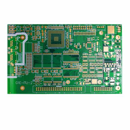
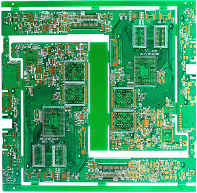
PCB board
Common circuit boards are usually green, called PCB board. In addition to green, common colors include blue, black, red, etc. PCB board is provided with bonding pads, wiring, vias, etc. The arrangement of bonding pads is consistent with the packaging of the chip. The chip and bonding pad can be welded together through soldering; The routing and via provide electrical connection. PCB board is shown in the figure below.
PCb board can be divided into double layer board, four layer board, six layer board and even more layers according to different layers. Most commonly used PCB board are made of FR-4 materials, with common thicknesses of 0.4mm, 0.6mm, 0.8mm, 1.0mm, 1.2mm, 1.6mm, 2.0mm, etc. This is a hard circuit board, and another is a soft circuit board, which is called a flexible circuit board. For example, the flexible flat cable of mobile phones and computers is a flexible pcb.
Welding tools
Soldering tools are needed to solder chips. For manual welding, tools such as electric soldering iron, solder wire and flux are required. Manual welding is applicable to a small number of sample plates, not suitable for mass production welding, because of low efficiency, poor consistency, solder skips, faulty soldering and other problems. Nowadays, the degree of mechanization is getting higher and higher, and the SMT mounting component welding is a very mature standardized industrial process. This process involves tin brushing machine, mounting machine, reflow soldering furnace, AOI detection and other equipment. The degree of automation is very high, the consistency is very good, and the error rate is very low, which ensures the mass shipment of electronic products. SMT can be said to be the infrastructure industry of the electronics industry.
Basic process of SMT
SMT is a standardized industrial process, involving PCB and incoming material inspection and verification, SMT loading, solder paste/red glue brushing, SMT pasting, over reflux furnace, AOI detection, cleaning and other processes. No mistakes can be made in any link. The incoming material check link mainly ensures the correctness of the materials. The placement position and direction of each component need to be determined by programming for the placement machine. Solder paste is applied to the bonding pad of PCB through the steel mesh. Reflow soldering is the process of heating and melting solder paste, and AOI is the detection process.
The chip is to be welded on the circuit board, which can not only fix the chip but also ensure the electrical connection between chips.
How to avoid FPC connector breakage?
Oct 26,2022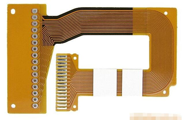


Just upload Gerber files, BOM files and design files, and the KINGFORD team will provide a complete quotation within 24h.