
Professional PCB manufacturing and assembly
Building 6, Zone 3, Yuekang Road,Bao'an District, Shenzhen, China
+86-13410863085Mon.-Sat.08:00-20:00


General process of PCB design:
Phase I: Scheme design:
In this stage, engineers usually plan the basic modules of the circuit and draw the circuit diagram of the product according to the situation of the circuit site, market research or product innovation needs. This stage can be completed without EDA design software. Manuscripts or other office software can generally meet the requirements. The following stages need to be applied to EDA design software.
The second stage: schematic design: in this stage, the specific schematic diagram is drawn according to the product circuit frame diagram to make the circuit system specific. The design in this stage will determine the circuit structure and PCB design wiring scale.
Stage 3: Export the component network table information to PCB design: After drawing the schematic diagram, the component packaging and pcb component connection information (called the network table) needs to be transferred to the PCB environment. The current design software can directly send the component network table and component packaging information to the PCB design environment with a single command, and has seamless docking and two-way synchronization functions.
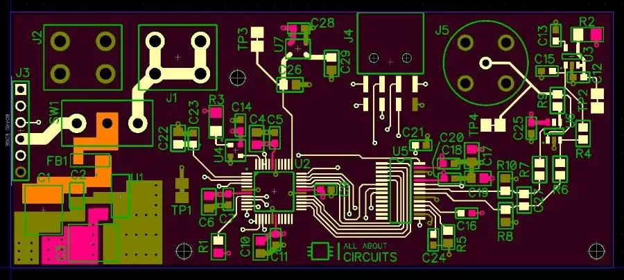
The fourth stage: component layout: after component packaging is transferred to the PCB design environment, component layout needs to be carried out according to the mold shape, panel structure, electromagnetic compatibility specifications, reasonable requirements for electrical layout, signal line impedance value requirements, PCB design stack structure and other characteristics of PCB products. This process is called component layout.
Stage 5: PCB wiring: after the components are arranged, according to the network table in the PCB design, the generated pre wiring needs to be filled with solid lines. This filler line is a copper foil line on the finished PCB. The rationality of PCB wiring will directly affect the quality of the PCB. Therefore, this stage is very important.
Stage 6: Computer aided manufacturing (CAM) processing and manufacturing: We do not need our electronic engineers to do this stage, but we need our electronic engineers to output GERBER files for processing and manufacturing.
Pcb layout is a problem that designers must face first. This problem depends on certain parts of the drawing, and some devices need to be set together according to logical considerations. However, it should be noted that temperature sensitive components (such as sensors) should be placed separately from heat generating components (including power converters). For designs with multiple power settings, 12 volt and 15 volt power converters can be placed at different locations on the board because the heat and electronic noise they generate can affect the reliability and performance of other components and boards.
Pcb board design solution
In the process of PCB design, many different methods can be used to solve various problems. It includes the adjustment of the design scheme itself, such as adjusting the circuit layout to reduce noise; And a layout method of a printed circuit board. You can use the layout tool to automatically install design components, but if you can manually adjust the automatic layout, it will help improve the quality of the board design. Through this measure, the design rule check will rely on technical documents to ensure that the circuit board design can meet the requirements of the circuit board manufacturer.


Just upload Gerber files, BOM files and design files, and the KINGFORD team will provide a complete quotation within 24h.