
Professional PCB manufacturing and assembly
Building 6, Zone 3, Yuekang Road,Bao'an District, Shenzhen, China
+86-13410863085Mon.-Sat.08:00-20:00

Multi-layer PCB production process
Compared with the particle board, the two most obvious advantages of the multi-layer board are: 1. The moisture resistance is better, because the fiber of the wood board is longer, and the moisture resistance of the board itself is better than that of the dispersed particles. 2. The theoretical glue is less than that of the particle board. Why is it called the theoretical glue? Because the shopping guide always says that the particle board is pressed in the glue after stirring, while the multi-layer board only applies a thin layer of glue on each layer of the board. , all with less glue. But this point of view is controversial, and a thin layer is actually not sticky. Moreover, the density of instant wood itself is very low, and its tube holes are relatively large, and it is easier to absorb glue, so even if there is really less glue, it is actually not much less.
The disadvantages are also obvious: 1. The precision is not as good as the particle board. The structure of the multi-layer board is made by pressing several layers of boards, because there are some errors in the slicing of the boards, the thickness of the glue, the sundries between the laminates and other factors, such as 18 thick For multi-layer boards, the plus or minus error may be 0.2-0.3MM, what will the error cause? For example, the gap between the door panels is large, and the cabinet body is not aligned when assembled, etc. 2. The edge banding is not as good as the particle board. The cross section of the multi-layer board is not as smooth as the particle board. In addition to the stress of the wood, its edge sealing is not as strong as the particle board.
Particle board:
A few days ago, downstairs in the community, I met a fellow who collected waste, and he was from a county. I was very happy to take the initiative to chat, because I live in a small third-tier city outside the city, and the chance of meeting fellow villagers is relatively small, so I chatted for a long time. During the chat, the fellow told me that our people, here, have made money a few years ago. They went to the construction site to collect the wood. It used to cost 800 yuan per ton. When the year is good, it can earn more than 300,000 yuan, but now it is not good. It is only two to three hundred yuan per ton, but now it can earn more than 100,000 yuan a year. Domestic anti-counterfeiting is not good enough, fake products are rampant, and there is a lack of supervision and management mechanisms. The cleverness of our compatriots is all used in these places. In the final analysis, it is not that the particle board is not good. After all, the domestic particle board is not good enough.
Kelifu leather board
Summary: Large manufacturers use particle board with high precision and suitable for standardized production. The advantage of small manufacturers lies in their flexibility. If particle boards are also used, how can they compete? It is better for us to adjust our thinking and make multi-layer boards for differentiation. How about particle board you ask them? Definitely not good.
In fact, the difference between the two is actually not so obvious, and both can meet family use. Generally, under the same material, the price of multi-layer boards is higher. My personal suggestion is to look at the price. If you can’t get over the hurdle in your heart, you can choose high-priced multi-layer boards. After reading the article, you think they are similar, and you can choose particle boards. But if you have come into contact with imported particle boards, I suggest you buy imported particle boards at the price of multi-layer boards.
【Overview】
The manufacture of multi-layer boards is to use several double-sided boards, and put an insulating layer between each board and stick them firmly (pressing). After each inner layer PCB has gone through AOI, and after the circuit pattern has been checked and confirmed to be correct, multiple PCBs need to be stacked together to form a multi-layer PCB. However, there are many things worth noting in this one. For example, it needs to be considered that the alignment of these double-sided panels must be ensured before being pressed together; it is also necessary to ensure that the bonding between the layers is firm. Therefore, before lamination, the following processes are required: [punching target holes], [browning], [PP punching], [stacking boards], and [pressing].
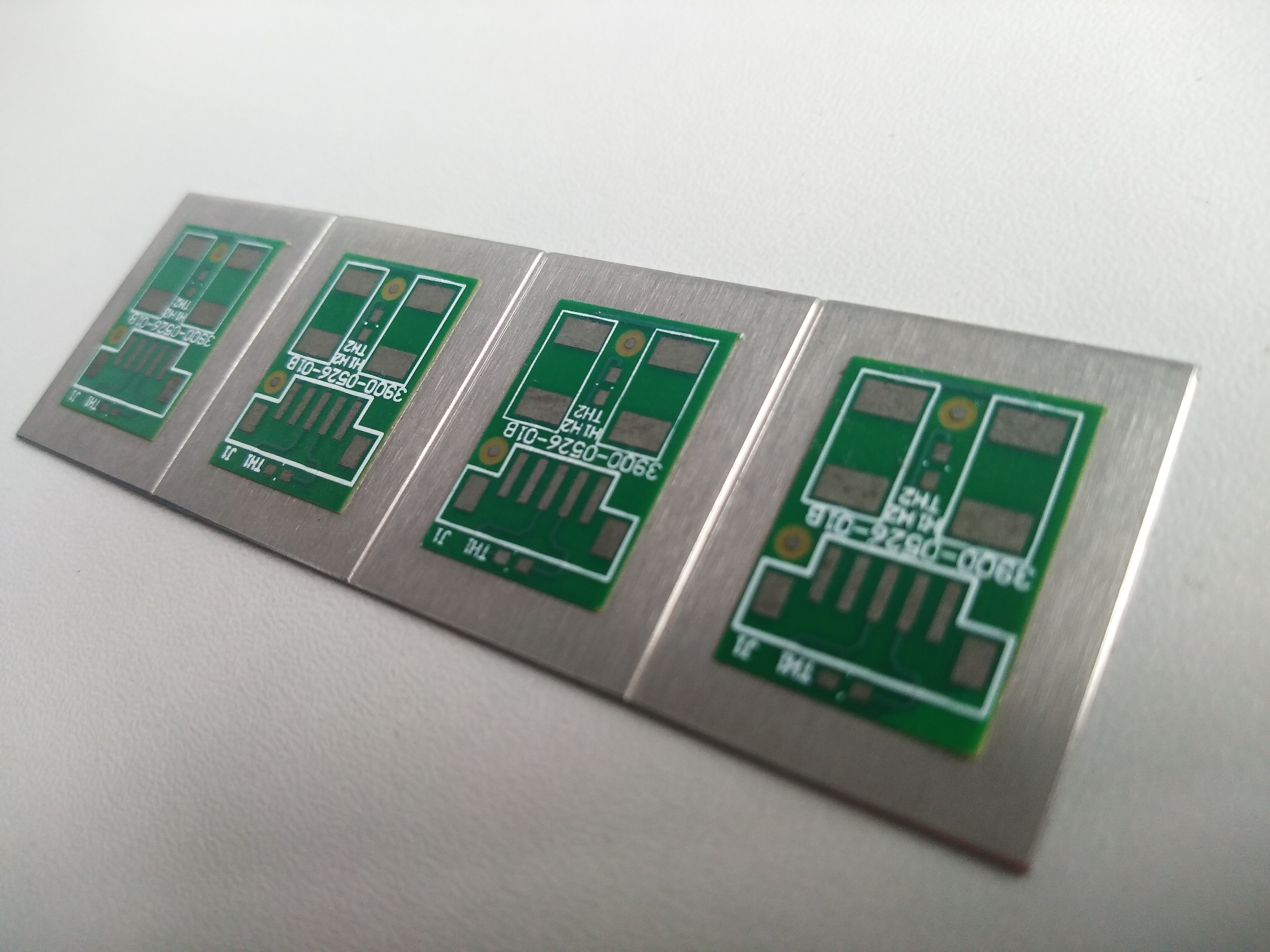
【Punch hole】
Before stacking and pressing, the inner boards need to be positioned and fixed by the target holes, so the rivet holes for pressing should be punched out by mechanical punching. The punching methods include OPE punching, CCD punching, and X-RAY shooting.
【Browning】
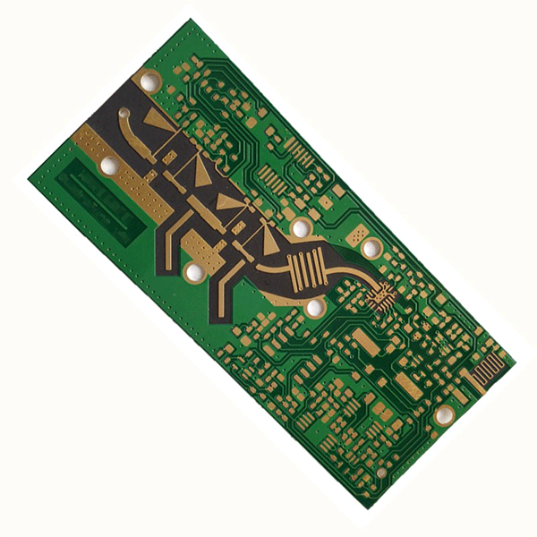
Before lamination, browning (also called blackening), this step is to treat the copper on the surface of the PCB that has been checked and confirmed to be correct (as shown in the figure below), so that the copper surface becomes fluffy and roughness is increased. An organic oxide layer is formed on the surface to increase the contact surface area with the resin and ensure reliable bonding of the laminate.
[PP sheet punching], [stacked plate]
In the step of stacking, there is no pressing yet. This step is to stack the multi-layer structures that need to be pressed in order. The schematic diagram of multi-layer PCB stack is as follows:
It can be seen from the above figure that in the structure of the laminated board, there are electrolytic copper skin, punched PP sheet (Prepreg) and browned single sheet. In fact, in addition to this, there are CVL (Coverlay, covering film, composed of insulating layer and adhesive <Adhesive>, as shown in the figure below, covering the wires for protection and insulation), RCC, release type
Once the stack is complete, it is ready for pressing. Lamination is a hot-pressing machine that presses heavily with steel plates on the PCB. After a certain period of time, the specified thickness is reached. After complete bonding, the bonding of the two PCB layers is considered complete.
So far, the multi-layer circuit board has been stacked together. Now, each layer has wires for each layer, however the layers are independent and there are no wires connecting them. Therefore, the next step is to drill holes on the board and drill via holes for circuit connections between layers.


Just upload Gerber files, BOM files and design files, and the KINGFORD team will provide a complete quotation within 24h.