
Professional PCB manufacturing and assembly
Building 6, Zone 3, Yuekang Road,Bao'an District, Shenzhen, China
+86-13410863085Mon.-Sat.08:00-20:00

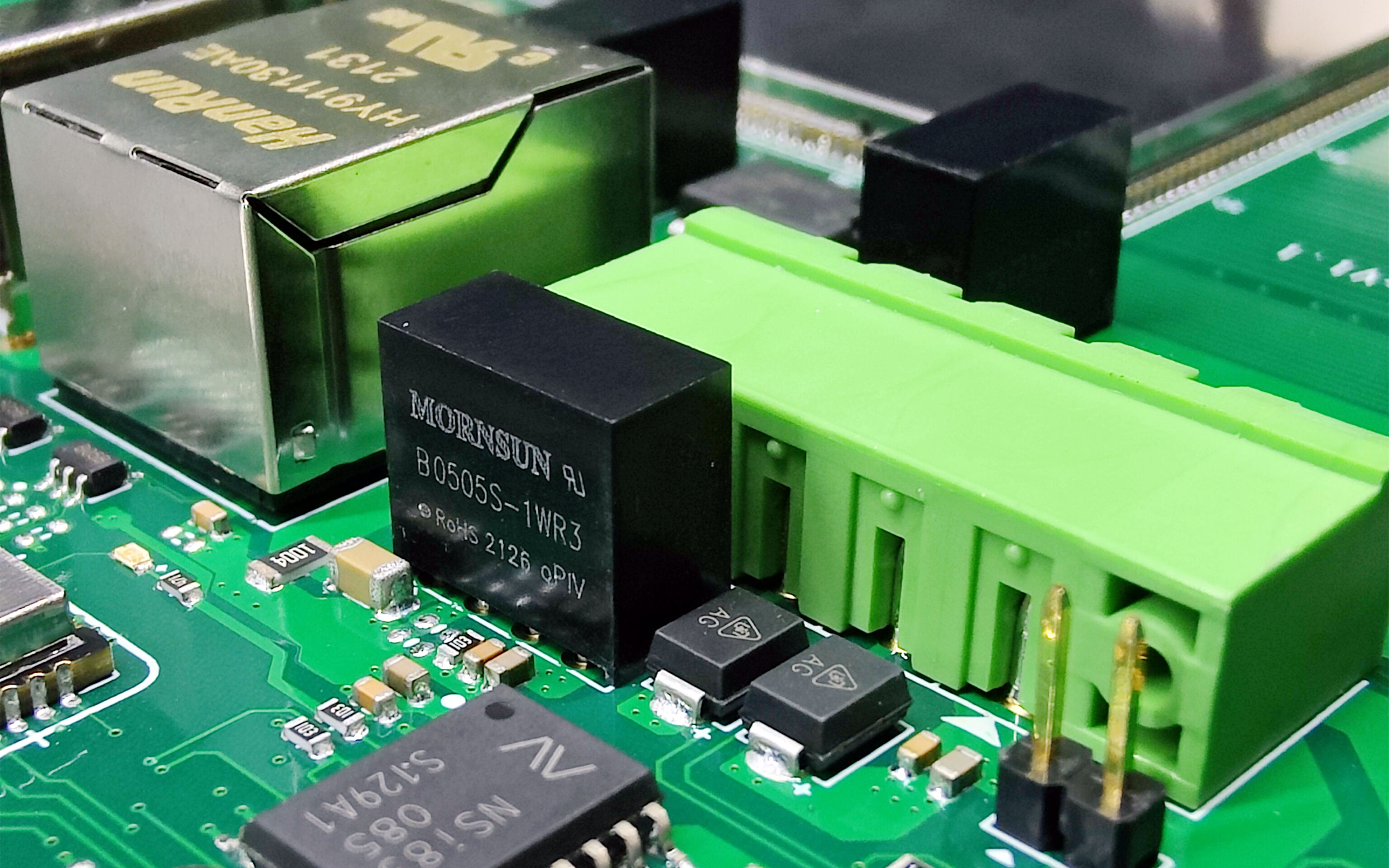
Significance and precautions of DIP plug-in processing
With the rapid development of SMT processing technology, SMT patch processing has gradually replaced DIP insertion processing. However, due to the oversize of some electronic components in PCBA production and other reasons, plug-in processing has not been replaced and still plays an important role in the electronic assembly process. DIP plug-in processing is after SMT patch processing, and generally uses assembly line manual plug-in, which requires a lot of employees.
The process flow of DIP plug-in processing can generally be divided into: device molding processing-plug-in-over-wave soldering-component leg cutting-repair soldering (post-soldering)-board cleaning-functional testing
1. Pre-processing the components
First of all, the staff in the pre-processing workshop go to the material place to pick up the materials according to the BOM material list, carefully check the material model, specification, sign, and perform pre-production pre-processing according to the model, using automatic bulk capacitor cutting machine, transistor automatic molding machine, fully automatic Forming equipment such as belt forming machines for processing.
2. Plug-ins
Insert the chip-processed components into the corresponding positions on the PCB board to prepare for wave soldering
3. Wave soldering
Put the inserted PCB board into the wave soldering conveyor belt, and complete the soldering of the PCB board after spraying flux, preheating, wave soldering, cooling and other links.
4. Component cutting feet
Cut the feet of the soldered PCBA board to achieve a suitable size.
5. Repair welding (post-welding)
For finished PCBA boards that have not been completely welded after inspection, repair welding should be carried out for maintenance.
6. Washing plate
Clean the harmful substances such as soldering flux remaining on the finished PCBA to meet the environmental protection standard cleanliness required by customers.
7. Function test
After the components are soldered, the finished PCBA board needs to be functionally tested to check whether the functions are normal. If a functional defect is detected, it needs to be repaired and retested.
DIP plug-in processing is a process in the processing of circuit boards with plug-in devices. According to different plug-in devices, it is divided into manual plug-in and machine plug-in.
What does DIP plug-in mean?
DIP package (Dual In-line Package), also known as dual in-line packaging technology, refers to integrated circuit chips packaged in dual in-line form. Most small and medium-sized integrated circuits use this package form. The number generally does not exceed 100. The DIP-packaged CPU chip has two rows of pins and needs to be inserted into a chip socket with a DIP structure. Of course, it can also be directly inserted into a circuit board with the same number of solder holes and geometric arrangement for soldering. When plugging and unplugging chips in DIP packages from the chip socket, special care should be taken to avoid damage to the pins. DIP package structures include: multi-layer ceramic dual in-line DIP, single-layer ceramic dual in-line DIP, lead frame DIP (including glass ceramic sealing type, plastic encapsulation structure type, ceramic low-melting glass encapsulation type) wait.
Precautions for DIP plug-in processing
1. Wear protective equipment such as electrostatic wristbands and finger cots.
2. Prepare the materials in advance, put the received materials in the designated box, label them to prevent mixing materials, and preview in advance to familiarize yourself with the content of your work.
3. Insert the placed parts that need to be completed in this station into the corresponding pins on the PCB board, and pay attention to the front and back of the parts, and stick to the board surface.
4. Gently press the parts with your hands to ensure that the parts are placed in place, and check whether the parts have any errors such as floating height, skew, polarity, etc. 5. Check the inserted components and remove the wrong and defective components in time .
6. Due to manual errors and missed inspections, Jingbang Electronics has introduced the world's advanced and precise measurement technology, which can measure components from various angles to obtain 3D images, so as to perform damage safety and high-speed defect detection. It can quickly detect the plug-in height, position, wrong parts, missing parts, foreign objects, part lifting, BGA lifting, detection and other bad phenomena, which greatly improves the working efficiency of the plug-in.
7. Clean the dirty motherboard after the wave soldering oven.
8. Trim the parts with too long exposed corners, and be careful not to scratch the circuit board.
9. Quality requires inspection and testing of the motherboard to ensure that the defective rate of the product is reduced. In this way, a complete circuit board is produced.
SMT basic process
May 30,2023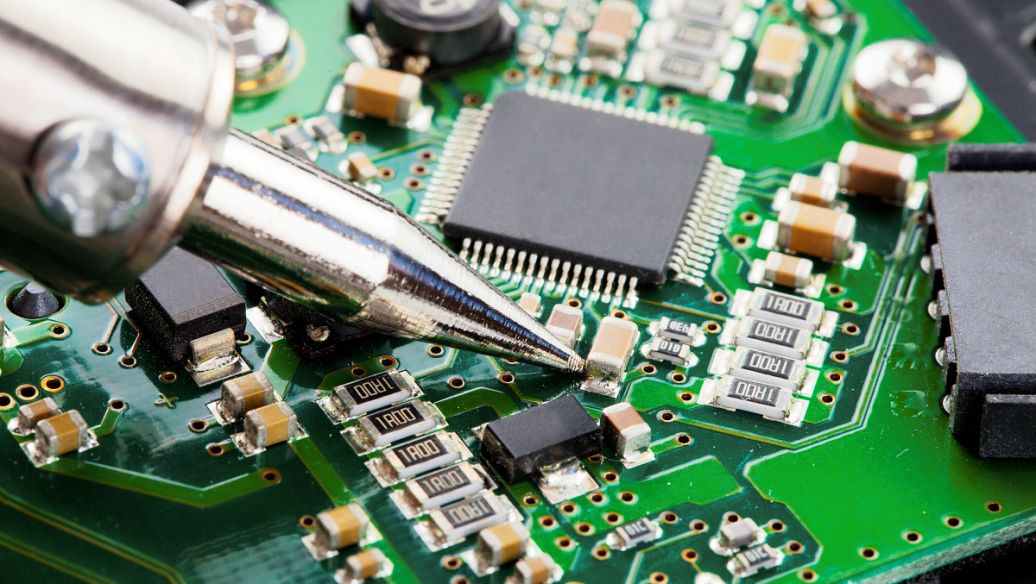


Just upload Gerber files, BOM files and design files, and the KINGFORD team will provide a complete quotation within 24h.